What is Global Gallium Nitride Single Crystal Substrates Market?
The Global Gallium Nitride (GaN) Single Crystal Substrates Market is a specialized segment within the broader semiconductor industry, focusing on the production and application of GaN substrates. These substrates are essential components used in the fabrication of various electronic and optoelectronic devices. GaN is a semiconductor material known for its superior properties, such as high thermal conductivity, high breakdown voltage, and high electron mobility, making it ideal for high-power and high-frequency applications. The market for GaN single crystal substrates is driven by the increasing demand for efficient and compact electronic devices, particularly in sectors like telecommunications, automotive, and consumer electronics. As industries continue to seek materials that can enhance device performance while reducing energy consumption, GaN substrates are becoming increasingly popular. The market is characterized by ongoing research and development efforts aimed at improving the quality and reducing the cost of GaN substrates, which are crucial for the widespread adoption of GaN-based technologies. The growth of this market is also supported by the rising adoption of GaN in emerging applications such as electric vehicles and renewable energy systems, where efficiency and performance are critical.
in the Global Gallium Nitride Single Crystal Substrates Market:
In the Global Gallium Nitride Single Crystal Substrates Market, various types of substrates are utilized by different customers based on their specific needs and applications. The primary types of GaN substrates include GaN-on-Sapphire, GaN-on-Silicon Carbide (SiC), and GaN-on-Silicon. Each type has its unique advantages and is chosen based on factors such as cost, performance, and compatibility with existing manufacturing processes. GaN-on-Sapphire substrates are widely used due to their relatively low cost and established manufacturing processes. They are commonly employed in the production of LEDs and other optoelectronic devices. However, the thermal and electrical properties of sapphire are not as favorable as those of other substrates, which can limit the performance of the final device. GaN-on-Silicon Carbide substrates offer superior thermal conductivity and electrical performance, making them ideal for high-power and high-frequency applications. These substrates are often used in the production of power electronic devices and RF components. However, the high cost of SiC substrates can be a limiting factor for their widespread adoption. GaN-on-Silicon substrates are gaining popularity due to their cost-effectiveness and compatibility with existing silicon-based manufacturing infrastructure. They offer a good balance between performance and cost, making them suitable for a wide range of applications, including power electronics and RF devices. The choice of substrate type is also influenced by the specific requirements of the end application. For instance, in applications where thermal management is critical, such as high-power RF amplifiers, GaN-on-SiC substrates may be preferred due to their superior thermal properties. On the other hand, for applications where cost is a major consideration, such as consumer electronics, GaN-on-Silicon substrates may be more suitable. Additionally, the ongoing advancements in substrate technology are leading to the development of new types of GaN substrates, such as free-standing GaN substrates, which offer improved performance and reliability. These advancements are expected to further expand the range of applications for GaN substrates and drive the growth of the market. As the demand for high-performance electronic devices continues to grow, the Global Gallium Nitride Single Crystal Substrates Market is expected to witness significant growth, driven by the increasing adoption of GaN substrates across various industries.
LED, Laser Diodes, Power Electronic Devices, Others in the Global Gallium Nitride Single Crystal Substrates Market:
The usage of Global Gallium Nitride Single Crystal Substrates Market spans several key areas, including LEDs, laser diodes, power electronic devices, and other applications. In the LED industry, GaN substrates are crucial for the production of high-brightness and energy-efficient LEDs. The superior properties of GaN, such as high electron mobility and thermal conductivity, enable the production of LEDs with higher efficiency and longer lifespan compared to traditional materials. This makes GaN-based LEDs ideal for a wide range of applications, from general lighting to displays and automotive lighting. In the field of laser diodes, GaN substrates are used to produce blue and green laser diodes, which are essential components in various applications, including optical storage, laser projectors, and medical devices. The ability of GaN to operate at high frequencies and power levels makes it an ideal material for these applications, where performance and reliability are critical. In power electronic devices, GaN substrates are used to produce high-performance transistors and diodes that are capable of handling high voltages and currents. This makes them ideal for applications such as power converters, inverters, and RF amplifiers, where efficiency and performance are crucial. The superior thermal and electrical properties of GaN enable the production of smaller and more efficient power devices, which are essential for the development of compact and energy-efficient electronic systems. In addition to these applications, GaN substrates are also used in other areas, such as sensors and communication devices, where their unique properties can enhance performance and reliability. The ongoing advancements in GaN substrate technology are expected to further expand the range of applications and drive the growth of the market. As industries continue to seek materials that can enhance device performance while reducing energy consumption, the demand for GaN substrates is expected to increase, driving the growth of the Global Gallium Nitride Single Crystal Substrates Market.
Global Gallium Nitride Single Crystal Substrates Market Outlook:
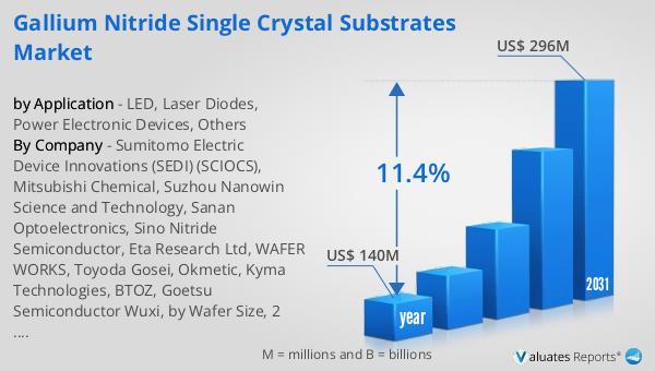
The global market for Gallium Nitride Single Crystal Substrates was valued at $140 million in 2024, and it is anticipated to grow significantly, reaching an estimated size of $296 million by 2031. This growth trajectory represents a compound annual growth rate (CAGR) of 11.4% over the forecast period. This impressive growth rate underscores the increasing demand for GaN substrates across various industries, driven by their superior properties and the growing need for high-performance electronic devices. The market's expansion is fueled by the rising adoption of GaN substrates in applications such as LEDs, laser diodes, and power electronic devices, where their unique properties can enhance performance and efficiency. Additionally, the ongoing advancements in GaN substrate technology are expected to further drive market growth by enabling the development of new and improved products. As industries continue to seek materials that can enhance device performance while reducing energy consumption, the demand for GaN substrates is expected to increase, driving the growth of the Global Gallium Nitride Single Crystal Substrates Market. The market's growth is also supported by the increasing adoption of GaN in emerging applications such as electric vehicles and renewable energy systems, where efficiency and performance are critical.
| Report Metric | Details |
| Report Name | Gallium Nitride Single Crystal Substrates Market |
| Accounted market size in year | US$ 140 million |
| Forecasted market size in 2031 | US$ 296 million |
| CAGR | 11.4% |
| Base Year | year |
| Forecasted years | 2025 - 2031 |
| by Application |
|
| Production by Region |
|
| Consumption by Region |
|
| By Company | Sumitomo Electric Device Innovations (SEDI) (SCIOCS), Mitsubishi Chemical, Suzhou Nanowin Science and Technology, Sanan Optoelectronics, Sino Nitride Semiconductor, Eta Research Ltd, WAFER WORKS, Toyoda Gosei, Okmetic, Kyma Technologies, BTOZ, Goetsu Semiconductor Wuxi, by Wafer Size, 2 Inches, 4 Inches, Other |
| Forecast units | USD million in value |
| Report coverage | Revenue and volume forecast, company share, competitive landscape, growth factors and trends |


