What is Global Ultra Pure Copper Sputtering Target Market?
The Global Ultra Pure Copper Sputtering Target Market is a specialized segment within the materials industry, focusing on the production and distribution of ultra-pure copper targets used in sputtering processes. Sputtering is a technique used to deposit thin films of material onto a substrate, and it is essential in the manufacturing of various electronic components. Ultra-pure copper sputtering targets are crucial because they ensure high-quality film deposition, which is vital for the performance and reliability of electronic devices. These targets are used in industries such as semiconductors, electronics, and solar energy, where precision and purity are paramount. The market for these targets is driven by the increasing demand for advanced electronic devices and the need for efficient and reliable manufacturing processes. As technology continues to evolve, the demand for ultra-pure copper sputtering targets is expected to grow, driven by innovations in electronics and renewable energy sectors. The market is characterized by a focus on quality, with manufacturers striving to produce targets with the highest levels of purity to meet the stringent requirements of their customers. This emphasis on purity and quality is a key factor driving the growth and development of the Global Ultra Pure Copper Sputtering Target Market.
5N Purity, 6N Purity, Others in the Global Ultra Pure Copper Sputtering Target Market:
In the Global Ultra Pure Copper Sputtering Target Market, purity levels are a critical factor that determines the quality and performance of the sputtering targets. The terms 5N and 6N refer to the purity levels of the copper used in these targets, with 5N indicating 99.999% purity and 6N indicating 99.9999% purity. These high levels of purity are essential for applications that require precise and reliable thin film deposition. The 5N purity level is commonly used in applications where a high degree of purity is necessary, but the absolute highest level of purity is not required. This level of purity is sufficient for many electronic applications, providing a balance between performance and cost. On the other hand, 6N purity is used in applications where the utmost purity is required, such as in the production of high-performance semiconductors and advanced electronic devices. The higher purity level ensures that the deposited films have minimal impurities, which can significantly enhance the performance and reliability of the final product. In addition to 5N and 6N purity levels, there are other purity levels available in the market, catering to different needs and applications. These other purity levels may be used in less demanding applications or where cost considerations are a primary concern. The choice of purity level depends on the specific requirements of the application, with higher purity levels generally associated with higher costs. However, the benefits of using ultra-pure copper sputtering targets, such as improved performance and reliability, often outweigh the additional costs, making them a preferred choice for many high-tech applications. The demand for different purity levels in the Global Ultra Pure Copper Sputtering Target Market is influenced by various factors, including technological advancements, industry standards, and customer preferences. As technology continues to advance, the need for higher purity levels is expected to increase, driving the demand for 6N and other ultra-high purity targets. Manufacturers in this market are continually investing in research and development to improve the purity levels of their products and meet the evolving needs of their customers. This focus on innovation and quality is a key factor contributing to the growth and competitiveness of the Global Ultra Pure Copper Sputtering Target Market.
Integrated Circuits, Printed Circuit Boards, Solar Cells, Thin Film Deposition in the Global Ultra Pure Copper Sputtering Target Market:
The Global Ultra Pure Copper Sputtering Target Market plays a crucial role in several high-tech industries, including integrated circuits, printed circuit boards, solar cells, and thin film deposition. In the field of integrated circuits, ultra-pure copper sputtering targets are used to deposit thin copper films onto semiconductor wafers. This process is essential for creating the intricate circuitry required in modern electronic devices. The high purity of the copper ensures that the deposited films have excellent electrical conductivity and minimal defects, which are critical for the performance and reliability of integrated circuits. In printed circuit boards (PCBs), ultra-pure copper sputtering targets are used to create conductive pathways that connect different components on the board. The use of high-purity copper ensures that these pathways have low electrical resistance and high reliability, which are essential for the proper functioning of electronic devices. The demand for ultra-pure copper sputtering targets in the PCB industry is driven by the increasing complexity and miniaturization of electronic devices, which require more precise and reliable manufacturing processes. In the solar cell industry, ultra-pure copper sputtering targets are used to deposit thin copper films onto solar panels. These films play a crucial role in the efficiency and performance of solar cells, as they help to conduct electricity generated by the photovoltaic material. The high purity of the copper ensures that the films have excellent electrical conductivity and minimal defects, which are essential for maximizing the efficiency of solar cells. As the demand for renewable energy continues to grow, the use of ultra-pure copper sputtering targets in the solar cell industry is expected to increase. In thin film deposition, ultra-pure copper sputtering targets are used to create thin films of copper on various substrates. This process is used in a wide range of applications, including the production of optical coatings, magnetic storage media, and decorative coatings. The high purity of the copper ensures that the deposited films have excellent properties, such as high electrical conductivity, good adhesion, and minimal defects. The demand for ultra-pure copper sputtering targets in thin film deposition is driven by the increasing need for high-performance coatings in various industries. Overall, the Global Ultra Pure Copper Sputtering Target Market is essential for the production of high-quality electronic components and devices. The use of ultra-pure copper ensures that the deposited films have excellent properties, which are critical for the performance and reliability of the final products. As technology continues to advance, the demand for ultra-pure copper sputtering targets is expected to grow, driven by innovations in electronics, renewable energy, and other high-tech industries.
Global Ultra Pure Copper Sputtering Target Market Outlook:
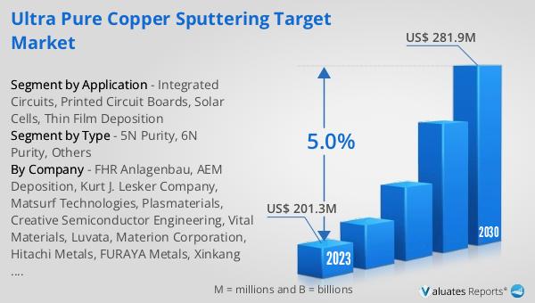
In 2024, the global market for Ultra Pure Copper Sputtering Targets was valued at approximately $220 million. This market is anticipated to expand significantly, reaching an estimated value of $308 million by the year 2031. This growth trajectory represents a compound annual growth rate (CAGR) of 5.0% over the forecast period. The increasing demand for high-purity copper sputtering targets is driven by the rapid advancements in technology and the growing need for efficient and reliable manufacturing processes in various industries. As electronic devices become more sophisticated and the demand for renewable energy sources rises, the need for ultra-pure copper sputtering targets is expected to increase. This market growth is also supported by the continuous innovation and development of new applications for sputtering targets, which are essential for the production of high-quality electronic components and devices. The focus on quality and purity in the production of sputtering targets is a key factor driving the growth of this market, as manufacturers strive to meet the stringent requirements of their customers. As a result, the Global Ultra Pure Copper Sputtering Target Market is poised for significant growth in the coming years, driven by the increasing demand for advanced electronic devices and the need for efficient and reliable manufacturing processes.
| Report Metric | Details |
| Report Name | Ultra Pure Copper Sputtering Target Market |
| Accounted market size in year | US$ 220 million |
| Forecasted market size in 2031 | US$ 308 million |
| CAGR | 5.0% |
| Base Year | year |
| Forecasted years | 2025 - 2031 |
| by Type |
|
| by Application |
|
| Production by Region |
|
| Consumption by Region |
|
| By Company | FHR Anlagenbau, AEM Deposition, Kurt J. Lesker Company, Matsurf Technologies, Plasmaterials, Creative Semiconductor Engineering, Vital Materials, Luvata, Materion Corporation, Hitachi Metals, FURAYA Metals, Xinkang Advanced Materials, Konfoong Materials International |
| Forecast units | USD million in value |
| Report coverage | Revenue and volume forecast, company share, competitive landscape, growth factors and trends |