What is Global Thick Layer Photoresists Market?
The Global Thick Layer Photoresists Market is a specialized segment within the broader photoresist industry, focusing on materials used in advanced semiconductor manufacturing processes. These photoresists are essential in creating intricate patterns on semiconductor wafers, which are crucial for producing microelectronic devices. Thick layer photoresists are particularly important in applications requiring high aspect ratio structures, such as microelectromechanical systems (MEMS), advanced packaging, and certain types of sensors. The market is driven by the increasing demand for miniaturized electronic devices and the need for more efficient and compact semiconductor components. As technology advances, the requirements for precision and performance in semiconductor manufacturing become more stringent, leading to a growing reliance on high-quality thick layer photoresists. The market is characterized by rapid technological advancements, with manufacturers continuously innovating to meet the evolving needs of the semiconductor industry. This dynamic environment presents both challenges and opportunities for companies operating in the global thick layer photoresists market, as they strive to balance cost, performance, and sustainability in their product offerings.
Thick Film Positive Photoresists, Thick Film Negative Photoresists in the Global Thick Layer Photoresists Market:
Thick Film Positive Photoresists and Thick Film Negative Photoresists are two primary types of photoresists used in the Global Thick Layer Photoresists Market, each serving distinct purposes and applications. Positive photoresists become soluble when exposed to light, allowing the exposed areas to be washed away during development. This property makes them ideal for applications requiring high-resolution patterning, as they can produce fine lines and intricate details. Positive photoresists are commonly used in the fabrication of integrated circuits and other microelectronic devices where precision is paramount. On the other hand, Thick Film Negative Photoresists work oppositely; they become insoluble when exposed to light, meaning the unexposed areas are removed during development. Negative photoresists are often used in applications where thicker layers are needed, such as in the creation of MEMS and certain types of sensors. They are valued for their ability to create robust, high-aspect-ratio structures that can withstand harsh processing conditions. Both types of photoresists are crucial in the semiconductor manufacturing process, each offering unique advantages depending on the specific requirements of the application. The choice between positive and negative photoresists often depends on factors such as the desired resolution, the thickness of the photoresist layer, and the specific processing conditions. As the demand for more advanced and miniaturized electronic devices continues to grow, the need for high-performance thick film photoresists is expected to increase, driving innovation and development in this specialized market segment. Manufacturers are continually working to improve the performance characteristics of both positive and negative photoresists, focusing on aspects such as sensitivity, resolution, and environmental impact. This ongoing innovation is essential to meet the ever-evolving demands of the semiconductor industry and to support the development of next-generation electronic devices.
Wafer-Level Packaging, Flip Chip (FC), Others in the Global Thick Layer Photoresists Market:
The Global Thick Layer Photoresists Market plays a crucial role in several advanced semiconductor manufacturing processes, including Wafer-Level Packaging, Flip Chip (FC), and other applications. Wafer-Level Packaging (WLP) is a technology that involves packaging integrated circuits while they are still part of the wafer, rather than after they have been cut into individual chips. This approach offers several advantages, including reduced package size, improved performance, and lower production costs. Thick layer photoresists are essential in WLP processes, as they enable the creation of precise patterns and structures needed for effective packaging. They provide the necessary thickness and resolution to support the complex designs required in modern electronic devices. Flip Chip (FC) technology is another area where thick layer photoresists are extensively used. FC involves mounting a semiconductor chip directly onto a substrate or circuit board, with the chip's active area facing down. This method allows for a higher density of connections and improved electrical performance compared to traditional wire bonding techniques. Thick layer photoresists are used in the FC process to create the bumps or pillars that connect the chip to the substrate, ensuring reliable and efficient electrical connections. In addition to WLP and FC, thick layer photoresists are used in various other applications, such as the fabrication of MEMS, sensors, and other microelectronic devices. These applications often require the creation of high-aspect-ratio structures, which can only be achieved with the use of high-quality thick layer photoresists. The versatility and performance of these materials make them indispensable in the production of advanced electronic components. As the demand for smaller, more powerful, and more efficient electronic devices continues to grow, the importance of thick layer photoresists in semiconductor manufacturing is expected to increase. Manufacturers are continually working to develop new formulations and improve existing products to meet the evolving needs of the industry. This ongoing innovation is essential to support the development of next-generation electronic devices and to maintain the competitiveness of the Global Thick Layer Photoresists Market.
Global Thick Layer Photoresists Market Outlook:
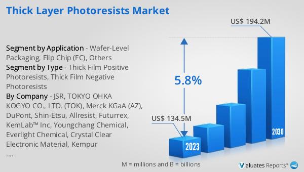
In 2024, the global market for Thick Layer Photoresists was valued at approximately $146 million. By 2031, it is anticipated to expand to a revised size of around $215 million, reflecting a compound annual growth rate (CAGR) of 5.8% over the forecast period. This growth trajectory underscores the increasing demand for thick layer photoresists, driven by advancements in semiconductor manufacturing and the rising need for miniaturized electronic devices. The market is dominated by a few key players, with the top three manufacturers collectively holding about 70% of the market share. Among these, Merck KGaA AZ stands out as the largest manufacturer, accounting for 25% of the market. This concentration of market share highlights the competitive nature of the industry and the importance of innovation and technological advancement in maintaining a leading position. As the market continues to evolve, companies are focusing on developing new products and improving existing ones to meet the changing needs of the semiconductor industry. This dynamic environment presents both challenges and opportunities for manufacturers, as they strive to balance cost, performance, and sustainability in their product offerings. The ongoing growth and development of the Global Thick Layer Photoresists Market are essential to support the advancement of next-generation electronic devices and to maintain the competitiveness of the semiconductor industry.
| Report Metric | Details |
| Report Name | Thick Layer Photoresists Market |
| Accounted market size in year | US$ 146 million |
| Forecasted market size in 2031 | US$ 215 million |
| CAGR | 5.8% |
| Base Year | year |
| Forecasted years | 2025 - 2031 |
| by Type |
|
| by Application |
|
| Production by Region |
|
| Consumption by Region |
|
| By Company | JSR, TOKYO OHKA KOGYO CO., LTD. (TOK), Merck KGaA (AZ), DuPont, Shin-Etsu, Allresist, Futurrex, KemLab™ Inc, Youngchang Chemical, Everlight Chemical, Crystal Clear Electronic Material, Kempur Microelectronics Inc, Xuzhou B & C Chemical |
| Forecast units | USD million in value |
| Report coverage | Revenue and volume forecast, company share, competitive landscape, growth factors and trends |


