What is Global Epoxy Molding Compound in Semiconductor Packaging Market?
Global Epoxy Molding Compound (EMC) in the semiconductor packaging market is a critical component used to encapsulate and protect semiconductor devices. These compounds are essential in safeguarding delicate electronic components from environmental factors such as moisture, dust, and mechanical stress. EMCs are thermosetting polymers that, once cured, form a hard, protective shell around the semiconductor chips. This encapsulation process not only enhances the durability and reliability of the semiconductor devices but also improves their thermal and electrical performance. The global demand for EMCs is driven by the rapid growth of the electronics industry, particularly in sectors like consumer electronics, automotive, and telecommunications. As devices become more compact and complex, the need for advanced packaging solutions like EMCs becomes increasingly important. The market is characterized by continuous innovation, with manufacturers striving to develop compounds that offer better performance, are environmentally friendly, and meet the stringent requirements of modern electronic applications. The global epoxy molding compound market is poised for significant growth, fueled by technological advancements and the increasing adoption of semiconductor devices across various industries.
Normal Epoxy Molding Compound, Green Epoxy Molding Compound in the Global Epoxy Molding Compound in Semiconductor Packaging Market:
Normal Epoxy Molding Compound (EMC) and Green Epoxy Molding Compound are two primary types of materials used in the semiconductor packaging industry, each serving distinct purposes and offering unique benefits. Normal EMCs are traditional compounds that have been used extensively in the industry for many years. They are composed of epoxy resins, hardeners, fillers, and other additives that provide the necessary mechanical and thermal properties required for semiconductor encapsulation. These compounds are known for their excellent adhesion, high thermal stability, and robust mechanical strength, making them suitable for a wide range of applications. However, traditional EMCs often contain halogens and other substances that can be harmful to the environment. This has led to the development of Green Epoxy Molding Compounds, which are designed to be more environmentally friendly. Green EMCs are formulated to reduce or eliminate the use of hazardous substances, such as halogens and antimony, without compromising on performance. They offer similar mechanical and thermal properties as their traditional counterparts but with a reduced environmental impact. The shift towards green EMCs is driven by increasing regulatory pressures and consumer demand for sustainable products. As a result, many manufacturers are investing in research and development to create innovative green compounds that meet the evolving needs of the semiconductor industry. The adoption of green EMCs is expected to grow as companies strive to reduce their carbon footprint and comply with environmental regulations. Both normal and green EMCs play a crucial role in the semiconductor packaging market, providing essential protection and performance enhancements for electronic devices. The choice between the two depends on various factors, including environmental considerations, performance requirements, and cost. As the industry continues to evolve, the demand for advanced EMCs that offer superior performance and sustainability is likely to increase, driving further innovation and growth in the market.
Advanced Packaging, Traditional Packaging in the Global Epoxy Molding Compound in Semiconductor Packaging Market:
The usage of Global Epoxy Molding Compound in Semiconductor Packaging Market spans across various packaging technologies, including Advanced Packaging and Traditional Packaging. Advanced Packaging refers to a set of techniques that enhance the performance and functionality of semiconductor devices beyond what is possible with conventional packaging methods. This includes technologies such as System-in-Package (SiP), Fan-Out Wafer-Level Packaging (FOWLP), and 3D packaging. In these applications, EMCs are used to encapsulate and protect the complex structures of advanced semiconductor devices. The compounds provide excellent thermal management, mechanical protection, and electrical insulation, which are critical for the reliable operation of high-performance devices. Advanced packaging solutions are increasingly being adopted in applications such as smartphones, tablets, and other high-end consumer electronics, where performance and miniaturization are key requirements. On the other hand, Traditional Packaging involves more conventional methods such as Dual In-line Package (DIP), Quad Flat Package (QFP), and Ball Grid Array (BGA). These techniques have been used for many years and remain popular due to their cost-effectiveness and reliability. In traditional packaging, EMCs are used to encapsulate semiconductor chips, providing protection against environmental factors and mechanical stress. The compounds help to ensure the longevity and reliability of the devices, making them suitable for a wide range of applications, including automotive, industrial, and consumer electronics. Despite the growing popularity of advanced packaging, traditional methods continue to hold a significant share of the market, particularly in applications where cost and simplicity are more important than performance. The choice between advanced and traditional packaging depends on various factors, including the specific requirements of the application, cost considerations, and the desired level of performance. As the semiconductor industry continues to evolve, the demand for both advanced and traditional packaging solutions is expected to grow, driving further innovation and development in the EMC market.
Global Epoxy Molding Compound in Semiconductor Packaging Market Outlook:
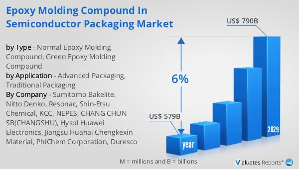
The global semiconductor market was valued at approximately $579 billion in 2022 and is anticipated to reach around $790 billion by 2029, reflecting a compound annual growth rate (CAGR) of 6% over the forecast period. This growth is indicative of the increasing demand for semiconductor devices across various industries, including consumer electronics, automotive, telecommunications, and industrial applications. The expansion of the semiconductor market is driven by several factors, including the proliferation of smart devices, the rise of the Internet of Things (IoT), and the growing adoption of advanced technologies such as artificial intelligence (AI) and 5G. As the demand for more powerful and efficient semiconductor devices continues to rise, the need for advanced packaging solutions like epoxy molding compounds becomes increasingly important. EMCs play a crucial role in enhancing the performance, reliability, and longevity of semiconductor devices, making them an essential component of the packaging process. The market outlook for epoxy molding compounds in semiconductor packaging is positive, with significant growth opportunities driven by technological advancements and the increasing adoption of semiconductor devices across various industries. As the market continues to expand, manufacturers are likely to focus on developing innovative compounds that offer superior performance, sustainability, and cost-effectiveness to meet the evolving needs of the industry.
| Report Metric | Details |
| Report Name | Epoxy Molding Compound in Semiconductor Packaging Market |
| Accounted market size in year | US$ 579 billion |
| Forecasted market size in 2029 | US$ 790 billion |
| CAGR | 6% |
| Base Year | year |
| Forecasted years | 2025 - 2029 |
| by Type |
|
| by Application |
|
| Production by Region |
|
| Consumption by Region |
|
| By Company | Sumitomo Bakelite, Nitto Denko, Resonac, Shin-Etsu Chemical, KCC, NEPES, CHANG CHUN SB(CHANGSHU), Hysol Huawei Electronics, Jiangsu Huahai Chengkexin Material, PhiChem Corporation, Duresco |
| Forecast units | USD million in value |
| Report coverage | Revenue and volume forecast, company share, competitive landscape, growth factors and trends |


