Tuesday, October 22, 2024

Stereotactic Surgical Planning Software - Global Market Share and Ranking, Overall Sales and Demand Forecast 2024-2030

What is Stereotactic Surgical Planning Software - Global Market?

Stereotactic surgical planning software is a specialized tool used in the medical field to assist surgeons in planning and executing precise surgical procedures. This software is particularly valuable in neurosurgery, where accuracy is crucial due to the complexity and sensitivity of the brain and surrounding structures. The global market for this software is expanding as healthcare providers increasingly recognize its benefits in improving surgical outcomes. By integrating advanced imaging techniques, such as MRI and CT scans, the software allows surgeons to create detailed 3D models of a patient's anatomy. This enables them to plan the surgical approach with high precision, minimizing risks and improving the chances of success. The software also facilitates real-time navigation during surgery, providing surgeons with critical information to make informed decisions. As technology continues to advance, the demand for stereotactic surgical planning software is expected to grow, driven by the need for safer and more effective surgical interventions. The global market is witnessing increased adoption across various regions, with healthcare institutions investing in this technology to enhance their surgical capabilities and improve patient outcomes.

Stereotactic Surgical Planning Software - Market

Biopsy Planning, Deep Brain Stimulation (DBS), Others in the Stereotactic Surgical Planning Software - Global Market:

Stereotactic surgical planning software plays a crucial role in various medical procedures, including biopsy planning, deep brain stimulation (DBS), and other complex surgeries. In biopsy planning, the software aids in accurately targeting specific areas within the body to obtain tissue samples for diagnostic purposes. By utilizing detailed imaging data, the software helps surgeons identify the precise location of the biopsy site, reducing the risk of complications and ensuring that the sample is representative of the area of interest. This precision is particularly important in cases where the target area is small or located near critical structures. In the context of deep brain stimulation (DBS), stereotactic surgical planning software is instrumental in guiding the placement of electrodes within the brain. DBS is a treatment used for neurological conditions such as Parkinson's disease, essential tremor, and dystonia. The software assists in mapping the brain's intricate structures, allowing surgeons to determine the optimal trajectory for electrode insertion. This precision is vital to maximize the therapeutic benefits of DBS while minimizing potential side effects. Additionally, the software's ability to integrate with real-time imaging and navigation systems enhances the accuracy of electrode placement, contributing to improved patient outcomes. Beyond biopsy planning and DBS, stereotactic surgical planning software is utilized in a range of other procedures, including tumor resections, epilepsy surgery, and functional neurosurgery. In tumor resections, the software aids in delineating the boundaries of the tumor, helping surgeons achieve complete removal while preserving healthy tissue. This is particularly important in brain tumors, where preserving cognitive and motor functions is a priority. In epilepsy surgery, the software assists in identifying and targeting epileptogenic zones, enabling precise removal or disconnection of the affected areas. This can significantly reduce seizure frequency and improve the quality of life for patients with drug-resistant epilepsy. Functional neurosurgery, which encompasses procedures aimed at treating movement disorders and psychiatric conditions, also benefits from the precision offered by stereotactic surgical planning software. By accurately targeting specific brain regions, surgeons can achieve therapeutic effects while minimizing adverse outcomes. Overall, the versatility and precision of stereotactic surgical planning software make it an invaluable tool in modern medicine, contributing to safer and more effective surgical interventions across a wide range of applications.

Hospital, Ambulatory Surgery Center, Clinic in the Stereotactic Surgical Planning Software - Global Market:

The usage of stereotactic surgical planning software is prevalent in various healthcare settings, including hospitals, ambulatory surgery centers, and clinics. In hospitals, this software is an integral part of the neurosurgical department, where it is used to plan and execute complex brain surgeries. Hospitals often have access to advanced imaging technologies, such as MRI and CT scanners, which are essential for the software to create accurate 3D models of a patient's anatomy. The integration of these imaging modalities with the software allows neurosurgeons to plan surgical procedures with high precision, reducing the risk of complications and improving patient outcomes. In addition to neurosurgery, hospitals may also use stereotactic surgical planning software in other specialties, such as oncology and orthopedics, where precise surgical planning is critical. Ambulatory surgery centers, which focus on providing same-day surgical care, also benefit from the use of stereotactic surgical planning software. These centers often perform minimally invasive procedures that require precise targeting of specific areas within the body. The software's ability to integrate with real-time imaging and navigation systems enhances the accuracy of these procedures, allowing surgeons to achieve optimal results with minimal disruption to surrounding tissues. This precision is particularly important in ambulatory settings, where patients are expected to recover quickly and return home on the same day. By utilizing stereotactic surgical planning software, ambulatory surgery centers can offer high-quality care while minimizing the risk of complications and reducing recovery times. Clinics, particularly those specializing in neurology and neurosurgery, also utilize stereotactic surgical planning software to enhance their diagnostic and treatment capabilities. In a clinical setting, the software is often used for preoperative planning and consultation, allowing physicians to discuss surgical options with patients and provide detailed explanations of the planned procedure. This can help alleviate patient anxiety and improve understanding of the surgical process. Additionally, clinics may use the software to collaborate with other healthcare providers, sharing detailed surgical plans and imaging data to ensure continuity of care. Overall, the use of stereotactic surgical planning software across hospitals, ambulatory surgery centers, and clinics highlights its versatility and importance in modern healthcare. By enabling precise surgical planning and execution, the software contributes to improved patient outcomes and enhances the quality of care provided in various healthcare settings.

Stereotactic Surgical Planning Software - Global Market Outlook:

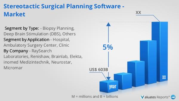
Based on our research, the global market for medical devices is projected to reach approximately $603 billion in 2023, with an anticipated growth rate of 5% annually over the next six years. This growth is driven by several factors, including advancements in medical technology, increasing demand for minimally invasive procedures, and the rising prevalence of chronic diseases. As healthcare systems worldwide continue to evolve, there is a growing emphasis on improving patient outcomes and reducing healthcare costs. Medical devices, including stereotactic surgical planning software, play a crucial role in achieving these goals by enabling precise and efficient surgical interventions. The expanding global market reflects the increasing adoption of advanced medical technologies across various regions, with healthcare providers investing in innovative solutions to enhance their capabilities. As the market continues to grow, it is expected to create new opportunities for manufacturers and developers of medical devices, driving further innovation and development in the field. The projected growth of the medical device market underscores the importance of continued investment in research and development to meet the evolving needs of healthcare providers and patients. By staying at the forefront of technological advancements, companies can capitalize on the growing demand for innovative medical solutions and contribute to the ongoing transformation of the healthcare industry.


Report Metric Details
Report Name Stereotactic Surgical Planning Software - Market
Accounted market size in year US$ 603 billion
CAGR 5%
Base Year year
Segment by Type:
  • Biopsy Planning
  • Deep Brain Stimulation (DBS)
  • Others
Segment by Application
  • Hospital
  • Ambulatory Surgery Center
  • Clinic
By Region
  • North America (United States, Canada)
  • Europe (Germany, France, UK, Italy, Russia) Rest of Europe
  • Nordic Countries
  • Asia-Pacific (China, Japan, South Korea)
  • Southeast Asia (India, Australia)
  • Rest of Asia
  • Latin America (Mexico, Brazil)
  • Rest of Latin America
  • Middle East & Africa (Turkey, Saudi Arabia, UAE, Rest of MEA)
By Company RaySearch Laboratories, Renishaw, Brainlab, Elekta, inomed Medizintechnik, Neurostar, Micromar
Forecast units USD million in value
Report coverage Revenue and volume forecast, company share, competitive landscape, growth factors and trends

Semiconductor Vacuum Soldering System - Global Market Share and Ranking, Overall Sales and Demand Forecast 2024-2030

What is Semiconductor Vacuum Soldering System - Global Market?

The semiconductor vacuum soldering system is a specialized technology used in the manufacturing and assembly of semiconductor devices. This system plays a crucial role in ensuring the reliability and performance of semiconductor components by providing a controlled environment for soldering processes. In the global market, semiconductor vacuum soldering systems are essential for producing high-quality electronic devices, as they help eliminate voids and defects in solder joints, which can lead to device failure. These systems are designed to operate under vacuum conditions, which reduces the presence of oxygen and other contaminants during the soldering process, resulting in stronger and more reliable connections. The demand for semiconductor vacuum soldering systems is driven by the increasing complexity and miniaturization of electronic devices, as well as the growing need for high-performance and energy-efficient semiconductors. As the global electronics industry continues to expand, the market for these systems is expected to grow, with manufacturers investing in advanced technologies to meet the evolving needs of the semiconductor sector. The semiconductor vacuum soldering system market is characterized by a diverse range of products and solutions, catering to various applications and industries, including consumer electronics, automotive, telecommunications, and industrial electronics.

Semiconductor Vacuum Soldering System - Market

Inline Type, Batch Type, Others in the Semiconductor Vacuum Soldering System - Global Market:

In the semiconductor vacuum soldering system market, there are several types of systems available, each designed to meet specific production needs and requirements. The inline type is one of the most common systems used in high-volume manufacturing environments. This type of system is integrated into the production line, allowing for continuous processing of semiconductor components. Inline systems are highly automated and offer high throughput, making them ideal for large-scale production. They are equipped with advanced features such as real-time monitoring and process control, ensuring consistent quality and efficiency. The batch type system, on the other hand, is designed for smaller production runs and is often used in research and development (R&D) settings. Batch systems are more flexible and can accommodate a wide range of component sizes and configurations. They are typically used for prototyping and testing new designs before scaling up to full production. Batch systems offer precise control over the soldering process, allowing for experimentation and optimization of parameters. Other types of semiconductor vacuum soldering systems include custom and hybrid solutions, which are tailored to meet specific customer requirements. These systems may combine elements of both inline and batch systems, offering a balance of flexibility and efficiency. Custom systems are often used in specialized applications where standard solutions may not be suitable. The choice of system type depends on various factors, including production volume, component complexity, and budget constraints. Manufacturers must carefully evaluate their needs and select the appropriate system to ensure optimal performance and cost-effectiveness. As the semiconductor industry continues to evolve, the demand for advanced soldering systems is expected to grow, with manufacturers seeking innovative solutions to meet the challenges of modern electronics production.

Batch Production, R&D in the Semiconductor Vacuum Soldering System - Global Market:

The semiconductor vacuum soldering system is widely used in batch production and research and development (R&D) settings, each with its unique requirements and challenges. In batch production, these systems are employed to produce semiconductor components in smaller quantities, often for specialized applications or niche markets. Batch production allows manufacturers to maintain flexibility and adapt to changing market demands, as it enables the production of different components without the need for extensive retooling or setup changes. Semiconductor vacuum soldering systems used in batch production are designed to handle a variety of component sizes and configurations, providing precise control over the soldering process. This flexibility is crucial for manufacturers who need to produce high-quality components with varying specifications. In R&D settings, semiconductor vacuum soldering systems are used to develop and test new semiconductor designs and technologies. R&D teams rely on these systems to experiment with different materials, processes, and configurations, allowing them to optimize performance and reliability. The ability to control the soldering environment and parameters is essential for R&D, as it enables researchers to identify and address potential issues before moving to full-scale production. Semiconductor vacuum soldering systems used in R&D are often equipped with advanced features such as real-time monitoring and data analysis, providing valuable insights into the soldering process. This information is critical for making informed decisions and improving the overall quality of semiconductor devices. The use of semiconductor vacuum soldering systems in both batch production and R&D highlights their importance in the semiconductor industry, as they enable manufacturers to produce high-performance components while maintaining flexibility and innovation.

Semiconductor Vacuum Soldering System - Global Market Outlook:

The global semiconductor market was valued at approximately $579 billion in 2022, and it is anticipated to reach around $790 billion by 2029, reflecting a compound annual growth rate (CAGR) of 6% over the forecast period. This growth is indicative of the increasing demand for semiconductors across various industries, driven by advancements in technology and the proliferation of electronic devices. The semiconductor industry is a critical component of the global economy, as semiconductors are essential for the functioning of a wide range of products, from consumer electronics to industrial machinery. The projected growth of the semiconductor market underscores the importance of continued innovation and investment in this sector, as manufacturers strive to meet the evolving needs of consumers and businesses. As the market expands, there will be increased opportunities for companies involved in the production and development of semiconductor technologies, including those specializing in semiconductor vacuum soldering systems. These systems play a vital role in ensuring the quality and reliability of semiconductor components, which are crucial for the performance of electronic devices. The growth of the semiconductor market is expected to drive demand for advanced soldering solutions, as manufacturers seek to enhance their production capabilities and maintain a competitive edge in the global market.


Report Metric Details
Report Name Semiconductor Vacuum Soldering System - Market
Accounted market size in year US$ 579 billion
Forecasted market size in 2029 US$ 790 billion
CAGR 6%
Base Year year
Forecasted years 2024 - 2029
Segment by Type:
  • Inline Type
  • Batch Type
  • Others
Segment by Application
  • Batch Production
  • R&D
By Region
  • North America (United States, Canada)
  • Europe (Germany, France, UK, Italy, Russia) Rest of Europe
  • Nordic Countries
  • Asia-Pacific (China, Japan, South Korea)
  • Southeast Asia (India, Australia)
  • Rest of Asia
  • Latin America (Mexico, Brazil)
  • Rest of Latin America
  • Middle East & Africa (Turkey, Saudi Arabia, UAE, Rest of MEA)
By Company Palomar Technologies, SMT Wertheim, PINK GmbH, budatec GmbH, centrotherm, Origin Co., Ltd., Rehm Thermal Systems, IBL Tech, Asscon, Shinko Seiki, Quick Intelligent, Heller Industries
Forecast units USD million in value
Report coverage Revenue and volume forecast, company share, competitive landscape, growth factors and trends

IC EDA Tools - Global Market Share and Ranking, Overall Sales and Demand Forecast 2024-2030

What is IC EDA Tools - Global Market?

IC EDA Tools, or Integrated Circuit Electronic Design Automation Tools, are specialized software applications used in the design and development of integrated circuits (ICs). These tools are essential for engineers and designers as they provide a comprehensive suite of functionalities to create, simulate, and test ICs before they are manufactured. The global market for IC EDA Tools is driven by the increasing demand for advanced electronics and the need for efficient design processes. These tools help in reducing the time and cost associated with IC design by automating various tasks such as schematic capture, layout design, and verification. As technology advances, the complexity of ICs increases, necessitating more sophisticated EDA tools to handle intricate designs. The market is also influenced by the growing trend of miniaturization in electronics, which requires precise and accurate design capabilities. With the rise of IoT devices, AI applications, and 5G technology, the demand for IC EDA Tools is expected to grow, as these sectors require highly efficient and reliable ICs. Overall, IC EDA Tools play a crucial role in the semiconductor industry, enabling the development of cutting-edge technology and innovation.

IC EDA Tools - Market

Analog Circuit, Digital Circuit, Flat Panel Display Circuit, Others in the IC EDA Tools - Global Market:

In the realm of IC EDA Tools, various types of circuits are designed and developed, each serving distinct purposes and applications. Analog circuits are fundamental components in electronics, dealing with continuous signals. They are crucial in applications where signal processing, amplification, and modulation are required. Analog circuits are used in devices like radios, audio equipment, and sensors, where they convert real-world signals into a form that can be processed by digital systems. The design of analog circuits using EDA tools involves creating precise and efficient layouts to ensure signal integrity and performance. On the other hand, digital circuits operate with discrete signals, representing data in binary form. These circuits are the backbone of modern computing and digital communication systems. EDA tools for digital circuits focus on logic design, simulation, and verification to ensure that the circuits perform as intended. Digital circuits are used in computers, smartphones, and digital communication devices, where they process and transmit data efficiently. Flat panel display circuits are another critical area in the IC EDA Tools market. These circuits are used in the design of displays for televisions, monitors, and mobile devices. The design process involves creating circuits that control the pixels on a display, ensuring high resolution and color accuracy. EDA tools help in optimizing the layout and performance of these circuits to meet the demands of modern display technology. Additionally, the IC EDA Tools market encompasses other specialized circuits, such as those used in power management, RF communication, and mixed-signal applications. Power management circuits are essential in managing the power consumption of electronic devices, ensuring efficiency and battery life. RF communication circuits are used in wireless communication systems, requiring precise design to handle high-frequency signals. Mixed-signal circuits combine analog and digital components, requiring sophisticated EDA tools to manage the complexities of integrating these different technologies. Overall, the IC EDA Tools market is diverse, catering to a wide range of circuit types and applications, each with its unique design challenges and requirements.

Automotive, Consumer Electronics, Communications, Medical, Aerospace and Defense, Industrial, Others in the IC EDA Tools - Global Market:

The usage of IC EDA Tools spans across various industries, each leveraging these tools to enhance their product development and innovation. In the automotive industry, IC EDA Tools are used to design and develop electronic control units (ECUs), sensors, and infotainment systems. These tools help in creating reliable and efficient circuits that are crucial for vehicle safety, performance, and connectivity. As the automotive industry moves towards electric and autonomous vehicles, the demand for advanced ICs and EDA tools is increasing. In consumer electronics, IC EDA Tools are essential for designing the circuits found in smartphones, tablets, and home appliances. These tools enable the development of compact and energy-efficient circuits that meet the high-performance demands of modern consumer devices. The communications industry relies heavily on IC EDA Tools for designing circuits used in networking equipment, mobile devices, and satellite systems. These tools help in creating circuits that support high-speed data transmission and connectivity. In the medical field, IC EDA Tools are used to design circuits for medical devices such as pacemakers, imaging equipment, and diagnostic tools. These circuits require high precision and reliability, which EDA tools help achieve through rigorous simulation and testing. The aerospace and defense industry uses IC EDA Tools to develop circuits for avionics, radar systems, and communication equipment. These applications require robust and reliable circuits that can withstand harsh environments and perform critical functions. In the industrial sector, IC EDA Tools are used to design circuits for automation systems, robotics, and industrial control systems. These tools help in creating efficient and reliable circuits that enhance productivity and operational efficiency. Additionally, IC EDA Tools find applications in other areas such as energy management, where they are used to design circuits for renewable energy systems and smart grids. Overall, IC EDA Tools are indispensable across various industries, enabling the development of innovative and efficient electronic solutions.

IC EDA Tools - Global Market Outlook:

The global semiconductor market, which was valued at approximately $579 billion in 2022, is anticipated to reach around $790 billion by 2029, reflecting a compound annual growth rate (CAGR) of 6% over the forecast period. This growth is indicative of the increasing demand for semiconductors across various industries, driven by advancements in technology and the proliferation of electronic devices. Semiconductors are the building blocks of modern electronics, found in everything from smartphones and computers to cars and industrial machinery. The growth of the semiconductor market is fueled by the rising adoption of technologies such as artificial intelligence, the Internet of Things (IoT), and 5G, which require advanced semiconductor solutions. Additionally, the trend towards miniaturization and the need for energy-efficient devices are driving innovation in semiconductor design and manufacturing. As the demand for semiconductors continues to rise, the market is expected to see significant investments in research and development, as well as in the expansion of manufacturing capabilities. This growth presents opportunities for companies involved in the semiconductor supply chain, from raw material suppliers to chip manufacturers and EDA tool providers. Overall, the semiconductor market is poised for substantial growth, driven by technological advancements and the increasing demand for electronic devices across various sectors.


Report Metric Details
Report Name IC EDA Tools - Market
Accounted market size in year US$ 579 billion
Forecasted market size in 2029 US$ 790 billion
CAGR 6%
Base Year year
Forecasted years 2024 - 2029
Segment by Type:
  • Analog Circuit
  • Digital Circuit
  • Flat Panel Display Circuit
  • Others
Segment by Application
  • Automotive
  • Consumer Electronics
  • Communications
  • Medical
  • Aerospace and Defense
  • Industrial
  • Others
By Region
  • North America (United States, Canada)
  • Europe (Germany, France, UK, Italy, Russia) Rest of Europe
  • Nordic Countries
  • Asia-Pacific (China, Japan, South Korea)
  • Southeast Asia (India, Australia)
  • Rest of Asia
  • Latin America (Mexico, Brazil)
  • Rest of Latin America
  • Middle East & Africa (Turkey, Saudi Arabia, UAE, Rest of MEA)
By Company Synopsys, Cadence, Siemens EDA, Ansys, Silvaco, Keysight Technologies, Empyrean Technology, Primarius Technologies, Zuken, Altium, National Instruments, Agnisys, Aldec, SMiT Holdings, Semitronix, Xpeedic Technology
Forecast units USD million in value
Report coverage Revenue and volume forecast, company share, competitive landscape, growth factors and trends

Semiconductor AOI Equipment - Global Market Share and Ranking, Overall Sales and Demand Forecast 2024-2030

What is Semiconductor AOI Equipment - Global Market?

Semiconductor Automated Optical Inspection (AOI) equipment is a crucial component in the global market for ensuring the quality and reliability of semiconductor devices. This equipment is designed to automatically inspect semiconductor wafers and printed circuit boards (PCBs) for defects during the manufacturing process. By using advanced imaging technologies, AOI systems can detect a wide range of defects, such as scratches, contamination, and misalignments, which are critical to maintaining the high standards required in semiconductor production. The global market for semiconductor AOI equipment is driven by the increasing demand for high-performance electronic devices, which necessitates stringent quality control measures. As technology advances, the complexity of semiconductor devices continues to grow, making AOI equipment indispensable for manufacturers aiming to minimize defects and improve yield rates. The market is characterized by continuous innovation, with manufacturers investing in research and development to enhance the capabilities of AOI systems, such as improving detection accuracy and reducing inspection times. This ongoing evolution ensures that AOI equipment remains a vital tool in the semiconductor industry, supporting the production of reliable and efficient electronic components.

Semiconductor AOI Equipment - Market

2D AOI, 3D AOI in the Semiconductor AOI Equipment - Global Market:

2D AOI and 3D AOI are two primary types of Automated Optical Inspection systems used in the semiconductor industry, each offering distinct advantages and applications. 2D AOI systems utilize high-resolution cameras to capture images of semiconductor wafers or PCBs from a single angle. These systems are adept at identifying surface-level defects, such as scratches, stains, or missing components, by comparing the captured images against predefined standards. The simplicity and cost-effectiveness of 2D AOI make it a popular choice for manufacturers who require basic inspection capabilities without the need for complex analysis. However, 2D AOI systems have limitations in detecting defects that involve height variations or are located beneath the surface, as they lack depth perception. On the other hand, 3D AOI systems employ advanced imaging techniques, such as structured light or laser triangulation, to create a three-dimensional representation of the inspected object. This capability allows 3D AOI systems to detect a broader range of defects, including those related to height, such as solder joint integrity or component coplanarity. The ability to measure height variations with high precision makes 3D AOI particularly valuable in applications where accurate dimensional analysis is critical. Despite being more complex and expensive than 2D AOI, 3D AOI systems offer superior inspection capabilities, making them indispensable for manufacturers seeking to ensure the highest quality standards. The choice between 2D and 3D AOI depends on the specific requirements of the manufacturing process, with factors such as defect types, inspection speed, and budget playing a crucial role in decision-making. As the semiconductor industry continues to evolve, the demand for more sophisticated AOI systems is expected to grow, driving further advancements in both 2D and 3D AOI technologies. Manufacturers are increasingly adopting 3D AOI systems to address the challenges posed by miniaturization and the increasing complexity of semiconductor devices. The integration of artificial intelligence and machine learning into AOI systems is also enhancing their capabilities, enabling more accurate defect detection and reducing false positives. This technological evolution is transforming AOI systems from simple inspection tools into comprehensive quality control solutions that can adapt to the dynamic needs of the semiconductor industry. As a result, both 2D and 3D AOI systems are playing a pivotal role in ensuring the reliability and performance of semiconductor devices, supporting the industry's growth and innovation.

PCB, Semiconductor Wafer, Others in the Semiconductor AOI Equipment - Global Market:

Semiconductor AOI equipment is extensively used in various areas, including Printed Circuit Boards (PCBs), semiconductor wafers, and other applications, to ensure the quality and reliability of electronic components. In the PCB manufacturing process, AOI systems are employed to inspect the boards for defects such as missing components, soldering issues, and misalignments. By using high-resolution cameras and advanced imaging techniques, AOI systems can quickly and accurately identify defects, allowing manufacturers to address issues before they escalate into larger problems. This capability is crucial in maintaining the high standards required in the production of PCBs, which serve as the backbone of electronic devices. In the context of semiconductor wafers, AOI equipment plays a vital role in inspecting the wafers for surface defects, contamination, and pattern misalignments. The ability to detect these defects early in the manufacturing process helps prevent costly rework and ensures that only high-quality wafers proceed to the next stages of production. AOI systems are also used in other areas, such as the inspection of microelectromechanical systems (MEMS) and optoelectronic devices, where precision and accuracy are paramount. The versatility of AOI equipment makes it an indispensable tool in the semiconductor industry, supporting the production of a wide range of electronic components. As technology continues to advance, the complexity of electronic devices increases, necessitating more sophisticated inspection solutions. AOI systems are evolving to meet these demands, with manufacturers investing in research and development to enhance their capabilities. The integration of artificial intelligence and machine learning into AOI systems is enabling more accurate defect detection and reducing false positives, further improving the efficiency of the inspection process. This ongoing innovation ensures that AOI equipment remains a critical component in the semiconductor industry, supporting the production of reliable and high-performance electronic devices.

Semiconductor AOI Equipment - Global Market Outlook:

The global semiconductor market was valued at approximately $579 billion in 2022 and is anticipated to reach around $790 billion by 2029, reflecting a compound annual growth rate (CAGR) of 6% over the forecast period. This growth trajectory underscores the increasing demand for semiconductors, driven by advancements in technology and the proliferation of electronic devices across various sectors. The semiconductor industry is a cornerstone of modern technology, providing the essential components that power everything from smartphones and computers to automobiles and industrial machinery. As the world becomes more interconnected and reliant on digital solutions, the demand for semiconductors is expected to continue its upward trend. This growth is further fueled by the emergence of new technologies, such as 5G, artificial intelligence, and the Internet of Things (IoT), which require advanced semiconductor solutions to function effectively. The projected expansion of the semiconductor market highlights the critical role that these components play in driving innovation and supporting the development of cutting-edge technologies. As the industry evolves, manufacturers are investing in research and development to enhance the performance and efficiency of semiconductor devices, ensuring that they can meet the growing demands of the digital age. This ongoing investment in innovation is essential for maintaining the competitiveness of the semiconductor industry and supporting its continued growth.


Report Metric Details
Report Name Semiconductor AOI Equipment - Market
Accounted market size in year US$ 579 billion
Forecasted market size in 2029 US$ 790 billion
CAGR 6%
Base Year year
Forecasted years 2024 - 2029
Segment by Type:
  • 2D AOI
  • 3D AOI
Segment by Application
  • PCB
  • Semiconductor Wafer
  • Others
By Region
  • North America (United States, Canada)
  • Europe (Germany, France, UK, Italy, Russia) Rest of Europe
  • Nordic Countries
  • Asia-Pacific (China, Japan, South Korea)
  • Southeast Asia (India, Australia)
  • Rest of Asia
  • Latin America (Mexico, Brazil)
  • Rest of Latin America
  • Middle East & Africa (Turkey, Saudi Arabia, UAE, Rest of MEA)
By Company Orbotech, Saki Corporation, Omron Corporation, Viscom, Marantz Electronics, Nordson, Koh Young Technology, Test Research, ViTrox, PARMI, Camtek, SCREEN Holdings, PEMTRON, AOI Systems, Mirtec, Utechzone, JUTZE Intelligence Technology, ZhenHuaXing, ALeader Europe, Vi Technology, Machine Vision Products, Sidea Semiconductor Equipment
Forecast units USD million in value
Report coverage Revenue and volume forecast, company share, competitive landscape, growth factors and trends

Semiconductor MOCVD Equipment - Global Market Share and Ranking, Overall Sales and Demand Forecast 2024-2030

What is Semiconductor MOCVD Equipment - Global Market?

Semiconductor MOCVD equipment is a crucial technology in the global market, primarily used for the deposition of thin films in the manufacturing of semiconductor devices. MOCVD stands for Metal-Organic Chemical Vapor Deposition, a process that allows for the precise layering of materials at the atomic level. This technology is essential for producing high-quality semiconductor wafers, which are the building blocks for a wide range of electronic devices. The global market for semiconductor MOCVD equipment is driven by the increasing demand for advanced electronic devices, such as smartphones, tablets, and other consumer electronics. Additionally, the rise of technologies like 5G, the Internet of Things (IoT), and electric vehicles has further fueled the need for efficient and high-performance semiconductor components. As a result, the MOCVD equipment market is experiencing significant growth, with manufacturers continuously innovating to meet the evolving demands of the semiconductor industry. This growth is also supported by the expansion of semiconductor manufacturing facilities worldwide, particularly in regions like Asia-Pacific, which is a major hub for electronics production. Overall, the semiconductor MOCVD equipment market plays a vital role in advancing technology and supporting the global electronics industry.

Semiconductor MOCVD Equipment - Market

GaN MOCVD, GaAs MOCVD, Others in the Semiconductor MOCVD Equipment - Global Market:

Gallium Nitride (GaN) and Gallium Arsenide (GaAs) are two prominent materials used in the semiconductor MOCVD equipment market, each offering unique advantages for various applications. GaN MOCVD is particularly valued for its high efficiency and power handling capabilities, making it ideal for power electronics, RF components, and LED production. GaN-based devices are known for their ability to operate at higher voltages and temperatures, which is crucial for applications in electric vehicles, renewable energy systems, and telecommunications. The demand for GaN MOCVD equipment is growing as industries seek to enhance the performance and efficiency of their electronic devices. On the other hand, GaAs MOCVD is widely used in the production of high-frequency and optoelectronic devices. GaAs materials are known for their superior electron mobility, which is essential for high-speed applications such as satellite communications, radar systems, and mobile networks. The GaAs MOCVD market is driven by the increasing need for high-performance communication systems and the growing adoption of advanced technologies like 5G. In addition to GaN and GaAs, other materials such as Indium Phosphide (InP) and Silicon Carbide (SiC) are also gaining traction in the semiconductor MOCVD equipment market. InP is particularly used in the production of high-speed and high-frequency devices, while SiC is favored for its robustness and efficiency in power electronics applications. The versatility of MOCVD technology allows for the deposition of these diverse materials, enabling the production of a wide range of semiconductor devices. As the demand for advanced electronic devices continues to rise, the semiconductor MOCVD equipment market is expected to expand further, driven by innovations in material science and deposition techniques. Manufacturers are investing in research and development to enhance the capabilities of MOCVD equipment, ensuring that it meets the stringent requirements of modern semiconductor manufacturing. This includes improving the precision and uniformity of thin film deposition, as well as increasing the throughput and efficiency of the equipment. The global semiconductor MOCVD equipment market is characterized by intense competition, with key players striving to gain a competitive edge through technological advancements and strategic partnerships. As the industry evolves, the focus is on developing sustainable and cost-effective solutions that can support the growing demand for high-performance semiconductor devices. Overall, the semiconductor MOCVD equipment market is poised for significant growth, driven by the increasing adoption of advanced materials and the continuous innovation in deposition technologies.

LED, Power Semiconductor, Laser Diode, Others in the Semiconductor MOCVD Equipment - Global Market:

Semiconductor MOCVD equipment is extensively used in various applications, including LED production, power semiconductors, laser diodes, and other advanced electronic devices. In the LED industry, MOCVD technology is crucial for the deposition of high-quality GaN layers, which are essential for producing efficient and bright LEDs. The demand for LEDs has surged in recent years due to their energy efficiency, long lifespan, and environmental benefits. MOCVD equipment enables manufacturers to produce LEDs with superior performance characteristics, catering to the growing demand for lighting solutions in residential, commercial, and industrial sectors. In the realm of power semiconductors, MOCVD equipment is used to deposit materials like GaN and SiC, which are known for their high efficiency and power handling capabilities. These materials are critical for the development of power electronic devices used in electric vehicles, renewable energy systems, and industrial applications. The ability of MOCVD technology to produce high-quality thin films with precise control over material properties is essential for enhancing the performance and reliability of power semiconductors. Laser diodes are another significant application of semiconductor MOCVD equipment. These devices are used in a wide range of applications, including telecommunications, medical devices, and consumer electronics. MOCVD technology allows for the deposition of materials like GaAs and InP, which are crucial for producing high-performance laser diodes with excellent optical and electrical properties. The demand for laser diodes is driven by the increasing need for high-speed data transmission, advanced imaging systems, and compact consumer electronics. Beyond these specific applications, semiconductor MOCVD equipment is also used in the production of various other electronic devices, such as photodetectors, solar cells, and sensors. The versatility of MOCVD technology enables manufacturers to produce a wide range of semiconductor devices with tailored properties, meeting the diverse needs of different industries. As the demand for advanced electronic devices continues to grow, the semiconductor MOCVD equipment market is expected to expand further, driven by innovations in deposition techniques and material science. Manufacturers are investing in research and development to enhance the capabilities of MOCVD equipment, ensuring that it meets the stringent requirements of modern semiconductor manufacturing. This includes improving the precision and uniformity of thin film deposition, as well as increasing the throughput and efficiency of the equipment. Overall, the semiconductor MOCVD equipment market plays a vital role in advancing technology and supporting the global electronics industry.

Semiconductor MOCVD Equipment - Global Market Outlook:

The global semiconductor market was valued at approximately $579 billion in 2022 and is anticipated to reach around $790 billion by 2029, reflecting a compound annual growth rate (CAGR) of 6% over the forecast period. This growth trajectory underscores the increasing demand for semiconductor devices across various industries, driven by technological advancements and the proliferation of electronic devices. The semiconductor industry is a cornerstone of modern technology, providing the essential components for a wide range of applications, from consumer electronics to industrial automation and telecommunications. The projected growth in the semiconductor market is fueled by the rising adoption of advanced technologies such as 5G, artificial intelligence, and the Internet of Things (IoT), which require sophisticated semiconductor components to function effectively. Additionally, the increasing demand for electric vehicles and renewable energy systems is driving the need for high-performance power semiconductors, further contributing to the market's expansion. As the semiconductor market continues to grow, manufacturers are investing in research and development to enhance the performance and efficiency of their products, ensuring they meet the evolving needs of various industries. This includes the development of new materials and manufacturing processes, as well as the integration of advanced technologies like machine learning and automation into semiconductor production. Overall, the global semiconductor market is poised for significant growth, driven by the increasing demand for advanced electronic devices and the continuous innovation in semiconductor technology.


Report Metric Details
Report Name Semiconductor MOCVD Equipment - Market
Accounted market size in year US$ 579 billion
Forecasted market size in 2029 US$ 790 billion
CAGR 6%
Base Year year
Forecasted years 2024 - 2029
Segment by Type:
  • GaN MOCVD
  • GaAs MOCVD
  • Others
Segment by Application
  • LED
  • Power Semiconductor
  • Laser Diode
  • Others
By Region
  • North America (United States, Canada)
  • Europe (Germany, France, UK, Italy, Russia) Rest of Europe
  • Nordic Countries
  • Asia-Pacific (China, Japan, South Korea)
  • Southeast Asia (India, Australia)
  • Rest of Asia
  • Latin America (Mexico, Brazil)
  • Rest of Latin America
  • Middle East & Africa (Turkey, Saudi Arabia, UAE, Rest of MEA)
By Company Aixtron, Veeco, Taiyo Nippon Sanso, Advanced Micro-Fabrication Equipment, CVD Equipment Corporation, Annealsys, Agnitron Technology, NANO-MASTER
Forecast units USD million in value
Report coverage Revenue and volume forecast, company share, competitive landscape, growth factors and trends

Dog Dental Treats - Global Market Share and Ranking, Overall Sales and Demand Forecast 2024-2030

What is Dog Dental Treats - Global Market?

Dog dental treats are a specialized segment within the pet care industry, focusing on products designed to improve the oral health of dogs. These treats are formulated to help reduce plaque and tartar buildup, freshen breath, and promote overall dental hygiene. The global market for dog dental treats has been expanding due to increasing awareness among pet owners about the importance of oral health for their pets. As more people consider their pets as part of the family, they are more willing to invest in products that ensure their pets' well-being. This market is characterized by a variety of products, including chews, biscuits, and sticks, each designed to cater to different dog sizes and preferences. Additionally, the market is driven by innovations in product formulations, such as the inclusion of natural ingredients and the development of treats that cater to specific dietary needs, like gluten-free options. The growing trend of pet humanization, coupled with rising disposable incomes, particularly in emerging economies, is expected to further fuel the demand for dog dental treats globally. Manufacturers are also focusing on sustainable and eco-friendly packaging to appeal to environmentally conscious consumers. Overall, the dog dental treats market is poised for significant growth as pet owners continue to prioritize their pets' health and wellness.

Dog Dental Treats - Market

Gluten-Containing, Gluten-Free in the Dog Dental Treats - Global Market:

In the realm of dog dental treats, the distinction between gluten-containing and gluten-free products is becoming increasingly significant. Gluten, a protein found in wheat and other grains, can be a concern for some dogs, particularly those with sensitivities or allergies. As a result, the demand for gluten-free dog dental treats has been on the rise. These treats are formulated without wheat, barley, or rye, making them suitable for dogs with gluten intolerance. On the other hand, gluten-containing treats are still prevalent in the market, often favored for their texture and taste, which many dogs enjoy. The choice between gluten-containing and gluten-free treats often depends on the dog's dietary needs and the owner's preferences. For instance, some pet owners opt for gluten-free treats as a precautionary measure, even if their dogs do not exhibit any signs of gluten sensitivity. This trend is reflective of the broader human food market, where gluten-free products have gained popularity due to perceived health benefits. In terms of market dynamics, manufacturers are increasingly offering a diverse range of products to cater to both segments. This includes not only gluten-free options but also treats that are fortified with additional nutrients to support overall health. The packaging and marketing of these products often highlight their gluten-free status, appealing to health-conscious pet owners. Furthermore, the rise of e-commerce has made it easier for consumers to access a wide variety of dog dental treats, including niche products like gluten-free options. Online platforms provide detailed product information, allowing pet owners to make informed decisions based on their dogs' specific needs. The global market for dog dental treats is also influenced by regional dietary trends. In regions where gluten-free diets are more prevalent among humans, there is a corresponding increase in demand for gluten-free pet products. This has led to a proliferation of brands and products, each vying for a share of the growing market. Additionally, the emphasis on natural and organic ingredients in pet food is driving innovation in the gluten-free segment. Manufacturers are exploring alternative ingredients, such as sweet potatoes and chickpeas, to create gluten-free treats that are both nutritious and palatable. As the market continues to evolve, the competition between gluten-containing and gluten-free dog dental treats is likely to intensify, with manufacturers striving to meet the diverse needs of pet owners worldwide.

Small Dog, Medium Dog, Large Dog in the Dog Dental Treats - Global Market:

Dog dental treats are designed to cater to dogs of all sizes, including small, medium, and large breeds. Each size category has specific needs and preferences, which manufacturers consider when developing their products. For small dogs, dental treats are typically smaller in size and softer in texture to accommodate their delicate teeth and jaws. These treats are often formulated to be easily digestible, ensuring that they do not pose a choking hazard. Small dog owners often look for treats that are not only effective in promoting dental health but also appealing in taste, as smaller breeds can be more selective in their food choices. For medium-sized dogs, dental treats are designed to strike a balance between size and texture. These treats are often moderately firm, providing enough resistance to help clean teeth and massage gums without being too hard. Medium dog owners may prioritize treats that offer a combination of dental benefits and nutritional value, as these dogs are often more active and require a balanced diet. Large dogs, on the other hand, require dental treats that are robust and durable. These treats are typically larger and harder, designed to withstand the strong jaws and chewing power of bigger breeds. Large dog owners often seek out treats that can keep their pets engaged for longer periods, providing both dental benefits and mental stimulation. Across all size categories, the global market for dog dental treats is driven by the increasing awareness of the importance of oral health in dogs. Pet owners are becoming more proactive in preventing dental issues, such as gum disease and tooth decay, which can lead to more serious health problems if left untreated. As a result, there is a growing demand for dental treats that are tailored to the specific needs of different dog sizes. Manufacturers are responding to this demand by offering a wide range of products, each designed to cater to the unique requirements of small, medium, and large dogs. This includes not only variations in size and texture but also formulations that address specific health concerns, such as tartar control and breath freshening. The market for dog dental treats is also influenced by trends in pet ownership, with more people adopting dogs of various sizes and breeds. This diversity in the pet population is driving innovation and competition among manufacturers, who are constantly seeking to develop new and improved products to meet the evolving needs of pet owners. Overall, the usage of dog dental treats across different size categories is a key factor in the growth of the global market, as pet owners continue to prioritize their dogs' oral health and well-being.

Dog Dental Treats - Global Market Outlook:

The global market for medical devices, as per our research, is projected to reach a valuation of approximately $603 billion in 2023. This substantial market size underscores the critical role that medical devices play in the healthcare industry worldwide. Over the next six years, the market is expected to experience a steady growth rate, with a compound annual growth rate (CAGR) of 5%. This growth trajectory is indicative of the increasing demand for advanced medical technologies and innovations that enhance patient care and treatment outcomes. The expansion of the medical device market is driven by several factors, including the rising prevalence of chronic diseases, an aging global population, and the continuous advancements in medical technology. As healthcare systems around the world strive to improve patient outcomes and reduce costs, the adoption of cutting-edge medical devices is becoming increasingly essential. Furthermore, the growing emphasis on personalized medicine and minimally invasive procedures is fueling the demand for specialized medical devices. The market's growth is also supported by the increasing investments in research and development by key industry players, who are focused on developing innovative solutions to address unmet medical needs. Additionally, the regulatory landscape for medical devices is evolving, with governments and regulatory bodies implementing measures to ensure the safety and efficacy of these products. This has led to a more streamlined approval process, facilitating the entry of new and advanced devices into the market. As the global medical device market continues to expand, it presents significant opportunities for manufacturers, healthcare providers, and investors alike. The ongoing advancements in technology, coupled with the growing demand for high-quality healthcare, are expected to drive the market's growth in the coming years.


Report Metric Details
Report Name Dog Dental Treats - Market
Accounted market size in year US$ 603 billion
CAGR 5%
Base Year year
Segment by Type:
  • Gluten-Containing
  • Gluten-Free
Segment by Application
  • Small Dog
  • Medium Dog
  • Large Dog
By Region
  • North America (United States, Canada)
  • Europe (Germany, France, UK, Italy, Russia) Rest of Europe
  • Nordic Countries
  • Asia-Pacific (China, Japan, South Korea)
  • Southeast Asia (India, Australia)
  • Rest of Asia
  • Latin America (Mexico, Brazil)
  • Rest of Latin America
  • Middle East & Africa (Turkey, Saudi Arabia, UAE, Rest of MEA)
By Company Purina, Boehringer Ingelheim Animal Health, Tartar Shield, Milk-Bone, Pedigree, Oven-Baked Tradition, Greenies, Wellness Pet Company, Natural Dog Company, Indigenous Pet, Whimzees, Ilio Products, Merrick, ORAVET
Forecast units USD million in value
Report coverage Revenue and volume forecast, company share, competitive landscape, growth factors and trends

IC Design EDA Tools - Global Market Share and Ranking, Overall Sales and Demand Forecast 2024-2030

What is IC Design EDA Tools - Global Market?

IC Design EDA Tools, or Electronic Design Automation Tools, are specialized software applications used in the design and development of integrated circuits (ICs). These tools are essential for engineers and designers as they provide a comprehensive suite of functionalities to create, simulate, verify, and test IC designs before they are manufactured. The global market for IC Design EDA Tools is a dynamic and rapidly evolving sector, driven by the increasing demand for advanced semiconductor devices across various industries. As technology continues to advance, the complexity of IC designs has grown, necessitating more sophisticated EDA tools to ensure accuracy and efficiency in the design process. These tools help in reducing the time-to-market for new semiconductor products, enhancing design productivity, and minimizing errors. The market is characterized by continuous innovation, with companies investing heavily in research and development to offer cutting-edge solutions that cater to the ever-changing needs of the semiconductor industry. As a result, the IC Design EDA Tools market is poised for significant growth, driven by the proliferation of smart devices, the rise of the Internet of Things (IoT), and the increasing adoption of artificial intelligence and machine learning technologies.

IC Design EDA Tools - Market

Circuit Simulation EDA Tool, Circuit Verification EDA Tool, Others in the IC Design EDA Tools - Global Market:

Circuit Simulation EDA Tools are a crucial component of the IC Design EDA Tools market, providing engineers with the ability to model and analyze the behavior of electronic circuits before they are physically built. These tools allow designers to simulate the performance of circuits under various conditions, identify potential issues, and optimize designs for better efficiency and reliability. By using circuit simulation tools, engineers can experiment with different design configurations, test the impact of component variations, and ensure that the final product meets the desired specifications. This not only saves time and resources but also reduces the risk of costly errors in the manufacturing process. Circuit Verification EDA Tools, on the other hand, focus on ensuring that the design of an integrated circuit meets all the necessary specifications and standards. These tools perform rigorous checks to verify the functionality, performance, and reliability of the design, identifying any discrepancies or errors that need to be addressed before production. Verification tools are essential in the design process as they help in detecting design flaws early, preventing potential failures in the final product. Other EDA tools in the IC Design market include layout design tools, which assist in the physical design of the IC, and synthesis tools, which convert high-level design descriptions into gate-level representations. These tools work together to streamline the design process, improve design accuracy, and enhance overall productivity. The global market for IC Design EDA Tools is driven by the increasing complexity of semiconductor devices, the growing demand for high-performance electronics, and the need for faster time-to-market. As technology continues to evolve, the role of EDA tools in the design and development of integrated circuits becomes increasingly critical, making them indispensable in the semiconductor industry.

Automotive, Consumer Electronics, Communications, Medical, Aerospace and Defense, Industrial, Others in the IC Design EDA Tools - Global Market:

The usage of IC Design EDA Tools spans across various industries, each leveraging these tools to meet specific design and development needs. In the automotive industry, EDA tools are used to design and develop advanced electronic systems that enhance vehicle performance, safety, and efficiency. With the rise of electric vehicles and autonomous driving technologies, the demand for sophisticated semiconductor devices in the automotive sector has increased, driving the need for advanced EDA tools. In consumer electronics, EDA tools play a vital role in the design of compact, high-performance devices such as smartphones, tablets, and wearable technology. These tools enable designers to create complex integrated circuits that power modern consumer electronics, ensuring they meet the high standards of performance and reliability expected by consumers. In the communications industry, EDA tools are used to develop the semiconductor components that power telecommunications infrastructure, including 5G networks and data centers. These tools help in designing high-speed, reliable circuits that are essential for the seamless transmission of data across networks. In the medical field, EDA tools are used to design and develop advanced medical devices and equipment, such as imaging systems, diagnostic tools, and wearable health monitors. These tools ensure that medical devices are safe, reliable, and meet stringent regulatory standards. In the aerospace and defense sector, EDA tools are used to design and develop complex electronic systems that are critical for mission success. These tools help in creating robust, reliable circuits that can withstand harsh environments and meet the demanding requirements of aerospace and defense applications. In the industrial sector, EDA tools are used to design and develop semiconductor devices that power industrial automation systems, robotics, and other advanced manufacturing technologies. These tools help in creating efficient, reliable circuits that enhance productivity and operational efficiency. The global market for IC Design EDA Tools is driven by the increasing demand for advanced semiconductor devices across these industries, as well as the need for faster time-to-market and improved design productivity. As technology continues to evolve, the role of EDA tools in the design and development of integrated circuits becomes increasingly critical, making them indispensable in the semiconductor industry.

IC Design EDA Tools - Global Market Outlook:

The global semiconductor market was valued at approximately $579 billion in 2022, and it is anticipated to reach around $790 billion by 2029, reflecting a compound annual growth rate (CAGR) of 6% over the forecast period. This growth is indicative of the increasing demand for semiconductor devices across various industries, driven by technological advancements and the proliferation of smart devices. The semiconductor market is a key driver of innovation, enabling the development of new technologies and applications that enhance our daily lives. As the demand for high-performance, energy-efficient semiconductor devices continues to rise, the market is expected to experience significant growth in the coming years. The increasing adoption of artificial intelligence, machine learning, and the Internet of Things (IoT) is further fueling the demand for advanced semiconductor devices, driving the need for innovative solutions in the IC Design EDA Tools market. As a result, companies in the semiconductor industry are investing heavily in research and development to stay competitive and meet the evolving needs of their customers. The global semiconductor market is poised for continued growth, driven by the increasing demand for advanced technologies and the need for faster time-to-market.


Report Metric Details
Report Name IC Design EDA Tools - Market
Accounted market size in year US$ 579 billion
Forecasted market size in 2029 US$ 790 billion
CAGR 6%
Base Year year
Forecasted years 2024 - 2029
Segment by Type:
  • Circuit Simulation EDA Tool
  • Circuit Verification EDA Tool
  • Others
Segment by Application
  • Automotive
  • Consumer Electronics
  • Communications
  • Medical
  • Aerospace and Defense
  • Industrial
  • Others
By Region
  • North America (United States, Canada)
  • Europe (Germany, France, UK, Italy, Russia) Rest of Europe
  • Nordic Countries
  • Asia-Pacific (China, Japan, South Korea)
  • Southeast Asia (India, Australia)
  • Rest of Asia
  • Latin America (Mexico, Brazil)
  • Rest of Latin America
  • Middle East & Africa (Turkey, Saudi Arabia, UAE, Rest of MEA)
By Company Synopsys, Cadence, Siemens EDA, Ansys, Silvaco, Keysight Technologies, Empyrean Technology, Primarius Technologies, Zuken, Altium, National Instruments, Agnisys, Aldec, SMiT Holdings, Semitronix, Xpeedic Technology
Forecast units USD million in value
Report coverage Revenue and volume forecast, company share, competitive landscape, growth factors and trends

Global Physics Games Market Research Report 2025

What is Global Physics Games Market? The Global Physics Games Market is a dynamic and evolving sector within the broader gaming industry, c...