What is Global IEP and LEP Endpoint Detection System Market?
The Global IEP and LEP Endpoint Detection System Market is a specialized segment within the broader field of semiconductor manufacturing and process control. These systems are crucial for ensuring precision and efficiency in the production of semiconductor devices. The market encompasses technologies and solutions designed to detect endpoints during various stages of semiconductor fabrication, such as etching and thin film deposition. Endpoint detection systems are vital for optimizing production processes, reducing waste, and improving the quality of semiconductor products. The market is driven by the increasing demand for advanced semiconductor devices, which are essential components in a wide range of electronic products, from smartphones to automotive systems. As technology continues to advance, the need for more sophisticated and accurate endpoint detection systems grows, making this market an important area of focus for manufacturers and researchers alike. The market is characterized by continuous innovation and development, with companies investing in research and development to enhance the capabilities and accuracy of their endpoint detection systems. This ongoing evolution is expected to drive growth and expansion in the Global IEP and LEP Endpoint Detection System Market in the coming years.
IEP Endpoint Detection System, LEP Endpoint Detection System in the Global IEP and LEP Endpoint Detection System Market:
The IEP (Integrated Endpoint Detection) and LEP (Laser Endpoint Detection) systems are integral components of the semiconductor manufacturing process, each serving distinct yet complementary roles. IEP Endpoint Detection Systems are designed to integrate seamlessly into the semiconductor fabrication process, providing real-time monitoring and control. These systems utilize a variety of sensors and algorithms to detect the precise moment when a process step, such as etching or deposition, has reached its endpoint. This precision is crucial for ensuring that each layer of the semiconductor device is manufactured to exact specifications, minimizing defects and maximizing yield. IEP systems are particularly valued for their ability to provide continuous, in-situ monitoring, allowing for immediate adjustments to be made to the process as needed. This capability is essential in a manufacturing environment where even minor deviations can lead to significant quality issues. On the other hand, LEP Endpoint Detection Systems employ laser-based technologies to achieve similar objectives. These systems use laser beams to monitor changes in the material being processed, detecting subtle shifts that indicate the endpoint of a process step. LEP systems are known for their high sensitivity and accuracy, making them ideal for applications where precision is paramount. The use of laser technology allows for non-contact measurement, reducing the risk of contamination and damage to the delicate semiconductor materials. LEP systems are often used in conjunction with IEP systems, providing an additional layer of verification and control. The Global IEP and LEP Endpoint Detection System Market is driven by several key factors. The increasing complexity of semiconductor devices, with their ever-shrinking geometries and multi-layered structures, necessitates the use of advanced endpoint detection systems to ensure quality and efficiency. Additionally, the growing demand for consumer electronics, automotive electronics, and other high-tech products is fueling the need for more sophisticated semiconductor manufacturing processes. As a result, manufacturers are investing heavily in endpoint detection technologies to stay competitive and meet the demands of the market. Furthermore, the market is characterized by a high level of innovation and technological advancement. Companies are continually developing new and improved endpoint detection systems, incorporating cutting-edge technologies such as artificial intelligence and machine learning to enhance performance and accuracy. These advancements are expected to drive growth in the market, as manufacturers seek to leverage the latest technologies to improve their production processes. In conclusion, the IEP and LEP Endpoint Detection Systems play a critical role in the semiconductor manufacturing process, providing the precision and control needed to produce high-quality devices. The Global IEP and LEP Endpoint Detection System Market is poised for growth, driven by the increasing demand for advanced semiconductor devices and the ongoing development of new technologies. As the market continues to evolve, manufacturers and researchers will need to stay at the forefront of innovation to remain competitive and meet the needs of the industry.
Etching, Thin Film Deposition, Others in the Global IEP and LEP Endpoint Detection System Market:
The usage of Global IEP and LEP Endpoint Detection Systems in areas such as etching, thin film deposition, and others is pivotal to the semiconductor manufacturing process. In the etching process, endpoint detection systems are used to determine the precise moment when the etching process should be stopped. This is crucial because over-etching can damage the underlying layers of the semiconductor device, while under-etching can result in incomplete pattern transfer. IEP and LEP systems provide the accuracy and control needed to ensure that the etching process is completed correctly, minimizing defects and maximizing yield. The ability to detect endpoints accurately in real-time allows manufacturers to optimize their processes, reducing waste and improving efficiency. In thin film deposition, endpoint detection systems are used to monitor the thickness and uniformity of the deposited film. This is important because variations in film thickness can affect the performance and reliability of the semiconductor device. IEP and LEP systems provide the precision needed to ensure that the film is deposited to the correct specifications, improving the quality and consistency of the final product. The use of endpoint detection systems in thin film deposition also allows for real-time adjustments to be made to the process, ensuring that any deviations are corrected immediately. Beyond etching and thin film deposition, endpoint detection systems are used in a variety of other semiconductor manufacturing processes. For example, they are used in chemical mechanical planarization (CMP) to monitor the removal of material and ensure that the surface of the wafer is planarized to the correct specifications. They are also used in ion implantation to monitor the dose and energy of the implanted ions, ensuring that the process is completed accurately and efficiently. The use of endpoint detection systems in these processes is driven by the need for precision and control in semiconductor manufacturing. As devices become more complex and the demand for high-quality products increases, the need for advanced endpoint detection systems becomes more critical. Manufacturers are investing in these systems to improve their processes, reduce waste, and increase yield. The ability to detect endpoints accurately and in real-time allows manufacturers to optimize their processes, improving efficiency and reducing costs. In conclusion, the usage of Global IEP and LEP Endpoint Detection Systems in areas such as etching, thin film deposition, and others is essential to the semiconductor manufacturing process. These systems provide the precision and control needed to produce high-quality devices, minimizing defects and maximizing yield. As the demand for advanced semiconductor devices continues to grow, the need for sophisticated endpoint detection systems will only increase, driving further innovation and development in the market.
Global IEP and LEP Endpoint Detection System Market Outlook:
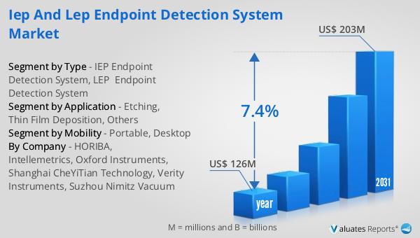
The worldwide market for IEP and LEP Endpoint Detection Systems was valued at $126 million in 2024. It is anticipated to expand to a revised size of $203 million by 2031, reflecting a compound annual growth rate (CAGR) of 7.4% over the forecast period. This growth trajectory underscores the increasing importance and demand for these systems in the semiconductor manufacturing industry. The projected growth is driven by several factors, including the rising complexity of semiconductor devices and the growing demand for high-quality electronic products. As technology continues to advance, the need for more sophisticated and accurate endpoint detection systems becomes increasingly critical. Manufacturers are investing in these systems to enhance their production processes, improve efficiency, and reduce costs. The market is characterized by continuous innovation and development, with companies striving to develop new and improved systems that incorporate the latest technologies. This ongoing evolution is expected to drive growth and expansion in the Global IEP and LEP Endpoint Detection System Market in the coming years. The market outlook highlights the significant opportunities for growth and development in this sector, as manufacturers and researchers work to meet the demands of the industry and stay at the forefront of technological innovation.
| Report Metric | Details |
| Report Name | IEP and LEP Endpoint Detection System Market |
| Accounted market size in year | US$ 126 million |
| Forecasted market size in 2031 | US$ 203 million |
| CAGR | 7.4% |
| Base Year | year |
| Forecasted years | 2025 - 2031 |
| Segment by Type |
|
| Segment by Mobility |
|
| Segment by Application |
|
| By Region |
|
| By Company | HORIBA, Intellemetrics, Oxford Instruments, Shanghai CheYiTian Technology, Verity Instruments, Suzhou Nimitz Vacuum |
| Forecast units | USD million in value |
| Report coverage | Revenue and volume forecast, company share, competitive landscape, growth factors and trends |


