What is Global Batch Wafer Cleaning System Market?
The Global Batch Wafer Cleaning System Market is a crucial segment within the semiconductor manufacturing industry, focusing on the cleaning of silicon wafers. These systems are essential for removing contaminants, particles, and residues from the wafer surfaces, ensuring the quality and performance of semiconductor devices. As the demand for smaller, more powerful electronic devices grows, the need for efficient wafer cleaning systems becomes increasingly important. The market encompasses a variety of cleaning technologies, including wet and dry batch cleaning systems, each offering unique advantages depending on the specific requirements of the semiconductor fabrication process. The market's growth is driven by advancements in semiconductor technology, increased production of integrated circuits, and the expansion of the electronics industry globally. With continuous innovations and the integration of advanced cleaning techniques, the Global Batch Wafer Cleaning System Market is poised to play a pivotal role in the future of semiconductor manufacturing, supporting the development of next-generation electronic devices.
Wet Batch Cleaning System, Dry Batch Cleaning System in the Global Batch Wafer Cleaning System Market:
In the realm of the Global Batch Wafer Cleaning System Market, two primary types of cleaning systems are prevalent: Wet Batch Cleaning Systems and Dry Batch Cleaning Systems. Wet Batch Cleaning Systems utilize liquid chemicals to clean the wafers. This method is highly effective in removing organic and inorganic contaminants, particles, and residues from the wafer surfaces. The process typically involves immersing the wafers in a series of chemical baths, followed by rinsing and drying. The advantage of wet cleaning lies in its ability to thoroughly clean the wafer surface, making it suitable for processes that require high levels of cleanliness. However, it also involves the use of large volumes of chemicals and water, which can lead to higher operational costs and environmental concerns. On the other hand, Dry Batch Cleaning Systems employ gaseous chemicals or plasma to clean the wafers. This method is advantageous in terms of reducing chemical and water usage, making it more environmentally friendly. Dry cleaning is particularly effective in removing particles and residues without the risk of watermarks or chemical residues. It is often used in processes where minimal contamination is critical, such as in the production of advanced semiconductor devices. Despite its benefits, dry cleaning may not be as effective as wet cleaning in removing certain types of contaminants, which can limit its application in some scenarios. Both wet and dry batch cleaning systems are integral to the semiconductor manufacturing process, each offering distinct benefits that cater to different stages of wafer processing. As the semiconductor industry continues to evolve, the demand for efficient and effective wafer cleaning solutions will drive further innovations in both wet and dry cleaning technologies, ensuring that they meet the stringent requirements of modern semiconductor fabrication.
Lithography Processes, Deposition Processes, Others in the Global Batch Wafer Cleaning System Market:
The Global Batch Wafer Cleaning System Market plays a vital role in various semiconductor manufacturing processes, including lithography and deposition, among others. In lithography processes, wafer cleaning systems are essential for preparing the wafer surface before the application of photoresist. A clean wafer surface ensures that the photoresist adheres properly, which is crucial for the accurate transfer of circuit patterns onto the wafer. Any contaminants or residues on the wafer surface can lead to defects in the circuit patterns, affecting the performance and yield of the semiconductor devices. Therefore, efficient wafer cleaning is critical in lithography to achieve high precision and quality in semiconductor manufacturing. In deposition processes, wafer cleaning systems are used to remove any particles or residues that may interfere with the deposition of thin films on the wafer surface. Clean wafer surfaces are essential for achieving uniform and defect-free thin films, which are crucial for the performance of semiconductor devices. Wafer cleaning systems help ensure that the deposition process is not compromised by contaminants, leading to improved device performance and reliability. Beyond lithography and deposition, wafer cleaning systems are also used in other semiconductor manufacturing processes, such as etching and chemical mechanical planarization (CMP). In etching, wafer cleaning is necessary to remove any residues left after the etching process, ensuring that the subsequent processing steps are not affected by contaminants. In CMP, wafer cleaning systems are used to remove slurry particles and residues from the wafer surface, ensuring a smooth and defect-free surface for further processing. Overall, the Global Batch Wafer Cleaning System Market is integral to the semiconductor manufacturing process, supporting various stages of wafer processing to ensure the production of high-quality and reliable semiconductor devices.
Global Batch Wafer Cleaning System Market Outlook:
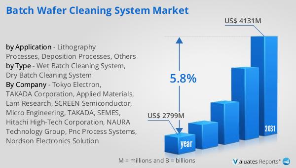
In 2024, the global market for Batch Wafer Cleaning Systems was valued at approximately $2,799 million. This market is anticipated to expand significantly, reaching an estimated size of $4,131 million by 2031. This growth trajectory represents a compound annual growth rate (CAGR) of 5.8% over the forecast period. The increasing demand for advanced semiconductor devices, driven by the proliferation of consumer electronics, automotive electronics, and the Internet of Things (IoT), is a key factor contributing to this market growth. As semiconductor manufacturers strive to enhance the performance and efficiency of their products, the need for effective wafer cleaning solutions becomes more pronounced. The adoption of innovative cleaning technologies and the integration of automation in wafer cleaning processes are expected to further propel market growth. Additionally, the expansion of semiconductor manufacturing facilities in emerging economies is likely to create new opportunities for market players. As the market evolves, companies are focusing on developing eco-friendly and cost-effective cleaning solutions to meet the growing demand for sustainable semiconductor manufacturing practices. Overall, the Global Batch Wafer Cleaning System Market is poised for substantial growth, driven by technological advancements and the increasing complexity of semiconductor devices.
| Report Metric | Details |
| Report Name | Batch Wafer Cleaning System Market |
| Accounted market size in year | US$ 2799 million |
| Forecasted market size in 2031 | US$ 4131 million |
| CAGR | 5.8% |
| Base Year | year |
| Forecasted years | 2025 - 2031 |
| by Type |
|
| by Application |
|
| Production by Region |
|
| Consumption by Region |
|
| By Company | Tokyo Electron, TAKADA Corporation, Applied Materials, Lam Research, SCREEN Semiconductor, Micro Engineering, TAKADA, SEMES, Hitachi High-Tech Corporation, NAURA Technology Group, Pnc Process Systems, Nordson Electronics Solution |
| Forecast units | USD million in value |
| Report coverage | Revenue and volume forecast, company share, competitive landscape, growth factors and trends |


