What is Global Wafer Holding and Transporting Vacuum Chuck Market?
The Global Wafer Holding and Transporting Vacuum Chuck Market is a specialized segment within the semiconductor industry that focuses on the devices used to hold and transport wafers during various stages of semiconductor manufacturing. These vacuum chucks are essential for maintaining the integrity and precision of wafers, which are thin slices of semiconductor material used in the fabrication of integrated circuits and other microdevices. The vacuum chuck operates by creating a vacuum seal that securely holds the wafer in place, preventing any movement that could lead to defects or misalignment during processing. This technology is crucial for ensuring high yields and the production of high-quality semiconductor devices. The market for these vacuum chucks is driven by the increasing demand for advanced semiconductor devices, the need for precision in manufacturing processes, and the continuous advancements in semiconductor technology. As the semiconductor industry continues to grow and evolve, the importance of reliable and efficient wafer handling and transporting solutions becomes even more critical.
200 mm, 300 mm, Others in the Global Wafer Holding and Transporting Vacuum Chuck Market:
In the Global Wafer Holding and Transporting Vacuum Chuck Market, wafers come in various sizes, with 200 mm and 300 mm being the most common, along with other sizes that cater to specific applications. The 200 mm wafers, also known as 8-inch wafers, have been a standard in the semiconductor industry for many years. They are widely used in the production of a variety of semiconductor devices, including microprocessors, memory chips, and sensors. The 200 mm wafer size offers a good balance between cost and performance, making it suitable for a wide range of applications. However, as the demand for more advanced and higher-performance semiconductor devices has increased, the industry has gradually shifted towards larger wafer sizes. The 300 mm wafers, or 12-inch wafers, represent the next step in this evolution. These larger wafers allow for more chips to be produced from a single wafer, significantly improving manufacturing efficiency and reducing costs. The transition to 300 mm wafers has been driven by the need for higher production volumes and the desire to achieve economies of scale. The larger wafer size also enables the use of more advanced manufacturing processes, which are essential for producing the latest generation of semiconductor devices. Despite the higher initial investment required for 300 mm wafer production, the long-term benefits in terms of cost savings and increased production capacity make it an attractive option for many semiconductor manufacturers. In addition to the standard 200 mm and 300 mm wafers, there are also other wafer sizes used in the industry, such as 150 mm (6-inch) and 450 mm (18-inch) wafers. The 150 mm wafers are typically used for older or specialized semiconductor processes, where the cost of upgrading to larger wafer sizes may not be justified. On the other hand, the 450 mm wafers represent the future of semiconductor manufacturing, offering even greater efficiencies and cost savings. However, the transition to 450 mm wafers has been slower due to the significant technical and financial challenges involved. The development of equipment and processes for handling and processing these larger wafers is still ongoing, and widespread adoption is expected to take several more years. The choice of wafer size in the Global Wafer Holding and Transporting Vacuum Chuck Market depends on various factors, including the specific requirements of the semiconductor devices being produced, the manufacturing capabilities of the semiconductor fabs, and the overall cost considerations. Each wafer size presents its own set of challenges and opportunities, and the industry continues to innovate and adapt to meet the evolving demands of the market. As semiconductor technology advances and new applications emerge, the need for efficient and reliable wafer handling and transporting solutions will remain a critical aspect of the semiconductor manufacturing process.
Wafer Suppliers, Semiconductor Equipment Suppliers in the Global Wafer Holding and Transporting Vacuum Chuck Market:
The Global Wafer Holding and Transporting Vacuum Chuck Market plays a crucial role in the operations of wafer suppliers and semiconductor equipment suppliers. For wafer suppliers, vacuum chucks are essential for ensuring the safe and precise handling of wafers throughout the manufacturing process. Wafers are delicate and highly sensitive to contamination, so maintaining their integrity is paramount. Vacuum chucks provide a secure and stable platform for holding wafers during various stages of production, including cleaning, inspection, and packaging. By preventing any movement or misalignment, vacuum chucks help to minimize the risk of defects and ensure that the wafers meet the stringent quality standards required by the semiconductor industry. Semiconductor equipment suppliers also rely heavily on vacuum chucks for the development and operation of their equipment. These suppliers design and manufacture the tools and machinery used in semiconductor fabrication, such as lithography systems, etching machines, and deposition equipment. Vacuum chucks are integrated into these systems to hold and transport wafers with precision and stability. The performance of the vacuum chuck directly impacts the overall efficiency and accuracy of the semiconductor manufacturing process. As such, equipment suppliers invest in advanced vacuum chuck technologies to enhance the capabilities of their equipment and meet the demands of their customers. In addition to their use in wafer handling and transportation, vacuum chucks are also employed in various testing and measurement applications within the semiconductor industry. For example, during wafer probing, vacuum chucks hold the wafer in place while electrical tests are conducted to verify the functionality of the semiconductor devices. Similarly, in metrology and inspection processes, vacuum chucks ensure that the wafer remains stable and accurately positioned for precise measurements and defect detection. The reliability and performance of vacuum chucks are critical for obtaining accurate test results and maintaining the overall quality of semiconductor products. The importance of vacuum chucks in the Global Wafer Holding and Transporting Vacuum Chuck Market extends beyond the manufacturing floor. They are also used in research and development (R&D) activities, where new semiconductor technologies and processes are being explored. In R&D labs, vacuum chucks provide the necessary stability and precision for experimenting with new materials, designs, and fabrication techniques. By enabling researchers to handle and manipulate wafers with accuracy, vacuum chucks contribute to the advancement of semiconductor technology and the development of innovative solutions for the industry. Overall, the Global Wafer Holding and Transporting Vacuum Chuck Market is integral to the operations of both wafer suppliers and semiconductor equipment suppliers. The technology ensures the safe and precise handling of wafers, which is essential for maintaining the quality and performance of semiconductor devices. As the semiconductor industry continues to evolve and demand for advanced devices grows, the role of vacuum chucks in supporting efficient and reliable manufacturing processes will remain vital.
Global Wafer Holding and Transporting Vacuum Chuck Market Outlook:
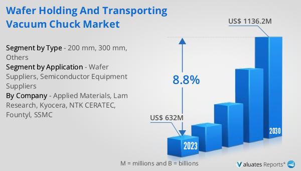
The global Wafer Holding and Transporting Vacuum Chuck market was valued at US$ 632 million in 2023 and is anticipated to reach US$ 1136.2 million by 2030, witnessing a CAGR of 8.8% during the forecast period 2024-2030. This market growth reflects the increasing demand for advanced semiconductor devices and the need for precision in manufacturing processes. The vacuum chuck technology is essential for maintaining the integrity and precision of wafers, which are critical components in the production of integrated circuits and other microdevices. As the semiconductor industry continues to grow and evolve, the importance of reliable and efficient wafer handling and transporting solutions becomes even more critical. The market for these vacuum chucks is driven by the continuous advancements in semiconductor technology and the increasing demand for high-quality semiconductor devices.
| Report Metric | Details |
| Report Name | Wafer Holding and Transporting Vacuum Chuck Market |
| Accounted market size in 2023 | US$ 632 million |
| Forecasted market size in 2030 | US$ 1136.2 million |
| CAGR | 8.8% |
| Base Year | 2023 |
| Forecasted years | 2024 - 2030 |
| Segment by Type |
|
| Segment by Application |
|
| Production by Region |
|
| Consumption by Region |
|
| By Company | Applied Materials, Lam Research, Kyocera, NTK CERATEC, Fountyl, SSMC |
| Forecast units | USD million in value |
| Report coverage | Revenue and volume forecast, company share, competitive landscape, growth factors and trends |


