Thursday, January 23, 2025

Global Display Driver Chip Packaging and Testing Market Insights, Forecast to 2030

What is Global Display Driver Chip Packaging and Testing Market?

The Global Display Driver Chip Packaging and Testing Market is a specialized segment within the semiconductor industry that focuses on the processes involved in preparing display driver chips for use in various electronic devices. Display driver chips are integral components that control the pixels on screens, enabling the display of images and videos on devices such as smartphones, tablets, televisions, and computer monitors. The packaging process involves encasing the chip in a protective shell to safeguard it from physical damage and environmental factors, while also facilitating its integration into electronic devices. Testing, on the other hand, ensures that these chips function correctly and meet the required performance standards before they are deployed in consumer products. This market is driven by the increasing demand for high-resolution displays and the proliferation of electronic devices across the globe. As technology advances, the need for more sophisticated and efficient display driver chips continues to grow, making packaging and testing crucial steps in the production process. The market is characterized by continuous innovation and the adoption of advanced technologies to enhance the performance and reliability of display driver chips.

Display Driver Chip Packaging and Testing Market

Chip Packaging, Chip Testing in the Global Display Driver Chip Packaging and Testing Market:

Chip packaging and testing are critical components of the Global Display Driver Chip Packaging and Testing Market, ensuring that display driver chips are ready for integration into electronic devices. Chip packaging involves several steps, starting with the selection of appropriate materials to encase the chip. The packaging must provide protection against physical damage, moisture, and other environmental factors while maintaining the chip's electrical performance. Various packaging techniques are employed, such as wire bonding, flip-chip, and wafer-level packaging, each offering different advantages in terms of size, cost, and performance. Wire bonding is a traditional method where fine wires connect the chip to the package, while flip-chip involves mounting the chip directly onto the substrate, allowing for better electrical performance and heat dissipation. Wafer-level packaging, on the other hand, is a more advanced technique that allows for smaller and thinner packages, ideal for compact devices. Once the chip is packaged, it undergoes rigorous testing to ensure its functionality and reliability. Testing is a multi-step process that includes electrical testing, thermal testing, and mechanical testing. Electrical testing verifies that the chip operates correctly under various conditions, checking for defects such as short circuits or open circuits. Thermal testing assesses the chip's ability to dissipate heat, ensuring it can operate within safe temperature ranges. Mechanical testing evaluates the chip's physical durability, ensuring it can withstand stresses such as vibration and impact. Advanced testing methods, such as automated test equipment (ATE) and built-in self-test (BIST) techniques, are employed to enhance testing efficiency and accuracy. The importance of chip packaging and testing cannot be overstated, as they directly impact the performance, reliability, and lifespan of display driver chips. As electronic devices become more sophisticated, the demand for high-quality display driver chips increases, driving innovation in packaging and testing technologies. Companies in this market are continually investing in research and development to improve packaging materials and testing methodologies, aiming to reduce costs and enhance chip performance. The integration of artificial intelligence and machine learning in testing processes is also gaining traction, offering the potential for more precise and efficient testing. In summary, chip packaging and testing are vital processes in the Global Display Driver Chip Packaging and Testing Market, ensuring that display driver chips meet the high standards required for modern electronic devices. These processes involve a combination of traditional and advanced techniques, with ongoing innovation aimed at improving efficiency and performance. As the demand for high-resolution displays and compact electronic devices continues to grow, the importance of effective chip packaging and testing will only increase, driving further advancements in this dynamic market.

Communication, Consumer Electronics, Vehicle Electronics, Aerospace, Other in the Global Display Driver Chip Packaging and Testing Market:

The Global Display Driver Chip Packaging and Testing Market plays a crucial role in various sectors, including communication, consumer electronics, vehicle electronics, aerospace, and others. In the communication sector, display driver chips are essential for devices such as smartphones, tablets, and smartwatches, which require high-quality displays for clear and vibrant visuals. The packaging and testing of these chips ensure that they can deliver the necessary performance and reliability, supporting the seamless operation of communication devices. As the demand for advanced communication technologies grows, the need for efficient display driver chips becomes increasingly important, driving innovation in packaging and testing processes. In the consumer electronics sector, display driver chips are used in a wide range of devices, including televisions, monitors, and gaming consoles. These devices require high-resolution displays to provide users with an immersive viewing experience. The packaging and testing of display driver chips ensure that they can meet the stringent performance standards required for consumer electronics, delivering crisp and clear images. As consumer preferences shift towards larger and more advanced displays, the demand for high-quality display driver chips continues to rise, highlighting the importance of effective packaging and testing. Vehicle electronics is another area where the Global Display Driver Chip Packaging and Testing Market is making a significant impact. Modern vehicles are equipped with various display systems, such as infotainment screens, digital dashboards, and rearview cameras, all of which rely on display driver chips. The packaging and testing of these chips ensure that they can withstand the harsh conditions of the automotive environment, including temperature fluctuations and vibrations. As the automotive industry moves towards more connected and autonomous vehicles, the demand for reliable display driver chips is expected to grow, emphasizing the need for robust packaging and testing solutions. In the aerospace sector, display driver chips are used in cockpit displays, navigation systems, and in-flight entertainment systems. These applications require chips that can operate reliably under extreme conditions, such as high altitudes and varying temperatures. The packaging and testing of display driver chips for aerospace applications ensure that they meet the rigorous standards required for safety and performance. As the aerospace industry continues to innovate, the demand for advanced display driver chips is likely to increase, driving further advancements in packaging and testing technologies. Beyond these sectors, the Global Display Driver Chip Packaging and Testing Market also serves other industries, such as healthcare and industrial automation, where display driver chips are used in medical imaging devices and control panels. The packaging and testing of these chips ensure that they can deliver the necessary performance and reliability, supporting the efficient operation of critical systems. As technology continues to evolve, the demand for high-quality display driver chips across various industries is expected to grow, underscoring the importance of effective packaging and testing processes.

Global Display Driver Chip Packaging and Testing Market Outlook:

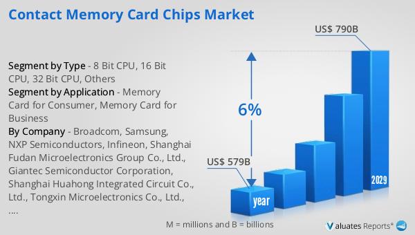
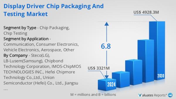
The outlook for the Global Display Driver Chip Packaging and Testing Market indicates a promising growth trajectory. The market is anticipated to expand from $3,321 million in 2024 to $4,928.3 million by 2030, reflecting a Compound Annual Growth Rate (CAGR) of 6.8% during the forecast period. This growth is driven by the increasing demand for advanced display technologies across various sectors, including consumer electronics, automotive, and aerospace. As electronic devices become more sophisticated, the need for high-performance display driver chips continues to rise, fueling the demand for efficient packaging and testing solutions. The broader semiconductor market, which was valued at $579 billion in 2022, is also projected to grow significantly, reaching $790 billion by 2029 with a CAGR of 6%. This growth underscores the importance of the Display Driver Chip Packaging and Testing Market within the semiconductor industry, as it plays a critical role in ensuring the quality and reliability of display driver chips. As technology continues to advance, the market is expected to witness further innovations in packaging and testing methodologies, enhancing the performance and efficiency of display driver chips. This positive outlook highlights the potential for continued growth and development in the Global Display Driver Chip Packaging and Testing Market, driven by the increasing demand for high-quality display technologies across various industries.


Report Metric Details
Report Name Display Driver Chip Packaging and Testing Market
Accounted market size in 2024 US$ 3321 million
Forecasted market size in 2030 US$ 4928.3 million
CAGR 6.8
Base Year 2024
Forecasted years 2025 - 2030
Segment by Type
  • Chip Packaging
  • Chip Testing
Segment by Application
  • Communication
  • Consumer Electronics
  • Vehicle Electronics
  • Aerospace
  • Other
By Region
  • North America (United States, Canada)
  • Europe (Germany, France, UK, Italy, Russia) Rest of Europe
  • Nordic Countries
  • Asia-Pacific (China, Japan, South Korea)
  • Southeast Asia (India, Australia)
  • Rest of Asia
  • Latin America (Mexico, Brazil)
  • Rest of Latin America
  • Middle East & Africa (Turkey, Saudi Arabia, UAE, Rest of MEA)
By Company Steco(LG), LB-Lusem(Samsung), Chipbond Technology Corporation, IMOS-ChipMOS TECHNOLOGIES INC., Hefei Chipmore Technology Co.,Ltd., Union Semiconductor (Hefei) Co., Ltd., Jiangsu Napace Semiconductor Co., Ltd., Tongfu Microelectronics Co.,ltd., JCET Group Co.,Ltd., ADVANCED SEMICONDUCTOR ENGINEERING, INC., Hitech Semiconductor (Wuxi) Co., Ltd., Hefei Chipmore Technology
Forecast units USD million in value
Report coverage Revenue and volume forecast, company share, competitive landscape, growth factors and trends

Global Portable Household Dehumidifier Market Insights, Forecast to 2030

What is Global Portable Household Dehumidifier Market?

The Global Portable Household Dehumidifier Market refers to the industry focused on the production and sale of portable devices designed to reduce humidity levels in residential spaces. These dehumidifiers are essential for maintaining indoor air quality, preventing mold growth, and ensuring comfort in homes, especially in regions with high humidity. The market encompasses a variety of dehumidifiers, each catering to different consumer needs and preferences. Factors driving the market include increasing awareness of health issues related to excessive humidity, technological advancements in dehumidifier design, and the growing demand for energy-efficient appliances. Additionally, the rise in disposable income and the expansion of the real estate sector contribute to the market's growth, as more homeowners seek to improve their living environments. The market is characterized by a diverse range of products, from basic models to advanced units with smart features, catering to a wide spectrum of consumers. As the demand for portable household dehumidifiers continues to rise, manufacturers are focusing on innovation and sustainability to meet consumer expectations and regulatory standards. This dynamic market is poised for significant growth, driven by the increasing need for effective humidity control solutions in homes worldwide.

Portable Household Dehumidifier Market

Condensation or Mechanical Refrigeration Dehumidifier, Hygroscopic Dehumidifier, Other in the Global Portable Household Dehumidifier Market:

Condensation or Mechanical Refrigeration Dehumidifiers are among the most common types of dehumidifiers used in households. These devices operate by drawing in moist air and passing it over a refrigerated coil. As the air cools, moisture condenses into water droplets, which are then collected in a tank or drained away. This process effectively reduces humidity levels in the air, making it more comfortable and healthier to breathe. These dehumidifiers are particularly effective in warm, humid climates where moisture levels are high. They are available in various sizes and capacities, allowing consumers to choose a model that best suits their needs. Hygroscopic Dehumidifiers, on the other hand, use materials that naturally absorb moisture from the air. These materials, known as desiccants, can be silica gel, activated alumina, or other hygroscopic substances. Unlike mechanical dehumidifiers, hygroscopic dehumidifiers do not rely on refrigeration, making them quieter and more energy-efficient. They are ideal for use in cooler climates or in spaces where noise is a concern, such as bedrooms or offices. Hygroscopic dehumidifiers are also portable and easy to maintain, as they do not require a compressor or refrigerant. Other types of dehumidifiers in the market include thermoelectric and ionic membrane dehumidifiers. Thermoelectric dehumidifiers use the Peltier effect to create a temperature difference across a semiconductor, causing moisture to condense on a cold surface. These dehumidifiers are compact and silent, making them suitable for small spaces. Ionic membrane dehumidifiers, meanwhile, use ionic membranes to separate water vapor from the air. These advanced devices are still relatively new to the market but offer promising potential for energy-efficient dehumidification. Each type of dehumidifier has its own advantages and limitations, and the choice of which to use depends on factors such as climate, space, and personal preferences. As technology continues to evolve, the Global Portable Household Dehumidifier Market is likely to see further innovations and improvements in dehumidifier design and functionality.

Online Sales, Offline Sales in the Global Portable Household Dehumidifier Market:

The Global Portable Household Dehumidifier Market serves a wide range of consumers through both online and offline sales channels. Online sales have become increasingly popular due to the convenience and accessibility they offer. Consumers can browse a vast selection of dehumidifiers from the comfort of their homes, compare prices, read reviews, and make informed purchasing decisions. E-commerce platforms and online retailers often provide detailed product descriptions, specifications, and customer feedback, helping buyers choose the right dehumidifier for their needs. Additionally, online sales often come with competitive pricing, discounts, and promotions, making them an attractive option for budget-conscious consumers. The rise of digital marketing and social media has further boosted online sales, as manufacturers and retailers can reach a broader audience and engage with potential customers through targeted advertising and interactive content. On the other hand, offline sales remain a significant part of the market, particularly for consumers who prefer a hands-on shopping experience. Physical stores allow customers to see and test dehumidifiers in person, providing a tactile experience that online shopping cannot replicate. Sales representatives in stores can offer personalized advice and recommendations, helping customers find the best product for their specific needs. Offline sales channels include appliance stores, home improvement centers, and department stores, where consumers can explore a variety of brands and models. Some consumers also prefer offline shopping for the immediate availability of products, as they can purchase and take home a dehumidifier on the same day. Both online and offline sales channels play a crucial role in the distribution of portable household dehumidifiers, catering to different consumer preferences and shopping habits. As the market continues to grow, manufacturers and retailers are likely to adopt an omnichannel approach, integrating both online and offline strategies to enhance customer experience and drive sales.

Global Portable Household Dehumidifier Market Outlook:

The outlook for the Global Portable Household Dehumidifier Market indicates a promising growth trajectory. The market is expected to expand from a valuation of approximately $2,309 million in 2024 to around $3,583.4 million by 2030. This growth is projected to occur at a Compound Annual Growth Rate (CAGR) of 7.6% over the forecast period. This upward trend reflects the increasing demand for effective humidity control solutions in residential settings. Several factors contribute to this growth, including rising awareness of the health benefits associated with maintaining optimal humidity levels, advancements in dehumidifier technology, and the growing emphasis on energy efficiency. As consumers become more conscious of indoor air quality and its impact on health, the demand for portable household dehumidifiers is likely to rise. Additionally, the expansion of the real estate sector and the increasing number of households worldwide further drive the market's growth. Manufacturers are focusing on innovation and sustainability to meet consumer expectations and regulatory standards, offering a diverse range of products with advanced features and improved energy efficiency. As a result, the Global Portable Household Dehumidifier Market is poised for significant growth, providing ample opportunities for industry players to capitalize on the increasing demand for humidity control solutions.


Report Metric Details
Report Name Portable Household Dehumidifier Market
Accounted market size in 2024 US$ 2309 million
Forecasted market size in 2030 US$ 3583.4 million
CAGR 7.6
Base Year 2024
Forecasted years 2025 - 2030
Segment by Type
  • Condensation or Mechanical Refrigeration Dehumidifier
  • Hygroscopic Dehumidifier
  • Other
Segment by Application
  • Online Sales
  • Offline Sales
Segment by Region
  • North America (United States, Canada)
  • Europe (Germany, France, UK, Italy, Russia) Rest of Europe
  • Nordic Countries
  • Asia-Pacific (China, Japan, South Korea)
  • Southeast Asia (India, Australia)
  • Rest of Asia
  • Latin America (Mexico, Brazil)
  • Rest of Latin America
  • Middle East & Africa (Turkey, Saudi Arabia, UAE, Rest of MEA)
By Company Songjing, Deve, Panasonic, TCL De'Longhi, Haier, Honeywell, Sharp, Frigidaire, Danby, LG Electronics, Dorosin, Mitsubishi Electric, Yadu, Aprilaire, Parkoo, Eurgeen, Philips, Friedrich, Hangzhou Dongma, Hangzhou Chuanjing Electrical Co., Ltd., Fudan Shenhua Purifying Technology Co.,Ltd.
Forecast units USD million in value
Report coverage Revenue and volume forecast, company share, competitive landscape, growth factors and trends

Global Road Noise Prevention Material Market Insights, Forecast to 2030

What is Global Road Noise Prevention Material Market?

The Global Road Noise Prevention Material Market refers to the industry focused on developing and supplying materials designed to reduce noise pollution from roadways. As urban areas expand and traffic volumes increase, road noise has become a significant environmental concern, affecting the quality of life for people living near busy roads. This market encompasses a variety of materials and technologies aimed at mitigating noise, including specialized asphalt, concrete, and other innovative solutions. These materials are engineered to absorb sound, reduce vibration, and minimize the transmission of noise from vehicles to surrounding areas. The demand for road noise prevention materials is driven by the need for quieter urban environments, regulatory requirements, and the growing awareness of the health impacts of noise pollution. As cities continue to grow and infrastructure projects expand, the market for these materials is expected to see significant growth, offering opportunities for companies involved in their production and application. The focus is on creating sustainable and effective solutions that not only address noise issues but also contribute to the overall durability and performance of road infrastructure.

Road Noise Prevention Material Market

Special Concrete, Noise-reducing Asphalt, Other in the Global Road Noise Prevention Material Market:

Special concrete is one of the key materials used in the Global Road Noise Prevention Material Market. This type of concrete is specifically designed to reduce noise by incorporating sound-absorbing properties. It often includes additives or aggregates that enhance its ability to dampen sound waves, making it an effective solution for reducing noise pollution in urban areas. Special concrete can be used in the construction of sound barriers, road surfaces, and other infrastructure elements where noise reduction is a priority. Its durability and versatility make it a popular choice for projects aiming to improve the acoustic environment of roadways. Noise-reducing asphalt is another critical component of this market. This type of asphalt is engineered to minimize the noise generated by tire-road interaction, which is a significant source of road noise. It typically features a porous structure that allows air to escape, reducing the sound produced by vehicles traveling over the surface. Noise-reducing asphalt is often used in high-traffic areas where noise pollution is a concern, providing a quieter and more pleasant environment for nearby residents. Other materials in the Global Road Noise Prevention Material Market include innovative solutions such as sound-absorbing panels, barriers, and coatings. These materials are designed to complement traditional road construction materials, offering additional noise reduction capabilities. Sound-absorbing panels and barriers are often installed alongside roadways to block and absorb noise, preventing it from reaching residential areas. Coatings can be applied to existing road surfaces to enhance their noise-reducing properties, providing a cost-effective solution for retrofitting older infrastructure. The development and application of these materials are driven by the need for sustainable and effective noise reduction solutions that can be integrated into modern road construction projects. As the demand for quieter urban environments continues to grow, the Global Road Noise Prevention Material Market is expected to expand, offering new opportunities for innovation and growth in the industry.

Construction, Transportation, Other in the Global Road Noise Prevention Material Market:

The usage of Global Road Noise Prevention Material Market in construction is primarily focused on integrating noise-reducing materials into the design and building of road infrastructure. This includes the use of special concrete and noise-reducing asphalt in the construction of roads, highways, and bridges. These materials are chosen for their ability to minimize noise pollution, enhancing the quality of life for people living near busy roadways. In addition to road surfaces, noise prevention materials are also used in the construction of sound barriers and walls, which are strategically placed to block and absorb noise from traffic. The construction industry plays a crucial role in implementing these materials, ensuring that new infrastructure projects meet the growing demand for quieter urban environments. In the transportation sector, the Global Road Noise Prevention Material Market is utilized to improve the acoustic performance of roadways, enhancing the overall experience for drivers and passengers. Noise-reducing materials are applied to road surfaces to decrease the noise generated by vehicles, creating a more pleasant and less stressful driving environment. This is particularly important in densely populated areas where traffic noise can be a significant source of stress and discomfort. By reducing road noise, transportation systems can operate more efficiently, with less impact on surrounding communities. Other applications of the Global Road Noise Prevention Material Market include the retrofitting of existing infrastructure to improve noise reduction capabilities. This involves the application of noise-reducing coatings and the installation of sound-absorbing panels and barriers on older roads and highways. These solutions provide a cost-effective way to address noise pollution in areas where new construction is not feasible. Additionally, noise prevention materials are used in various other settings, such as airports, railways, and industrial sites, where noise reduction is a priority. The versatility and effectiveness of these materials make them an essential component of efforts to create quieter and more sustainable environments.

Global Road Noise Prevention Material Market Outlook:

The outlook for the Global Road Noise Prevention Material Market indicates a promising growth trajectory. The market is anticipated to expand from a valuation of US$ 581 million in 2024 to approximately US$ 953.1 million by 2030. This growth is expected to occur at a Compound Annual Growth Rate (CAGR) of 8.6% over the forecast period. This upward trend reflects the increasing demand for noise reduction solutions in urban areas, driven by the expansion of cities and the rising awareness of the health impacts of noise pollution. As more people move to urban centers, the need for effective noise prevention materials becomes more critical, prompting investments in innovative technologies and materials. The market's growth is also supported by regulatory requirements aimed at reducing noise pollution and improving the quality of life in urban environments. Governments and municipalities are increasingly prioritizing noise reduction in their infrastructure projects, creating opportunities for companies involved in the production and application of road noise prevention materials. The focus is on developing sustainable and cost-effective solutions that can be integrated into existing and new road infrastructure, ensuring long-term benefits for communities. As the market continues to evolve, it is expected to see further advancements in material technology and application methods, enhancing the effectiveness and efficiency of noise reduction efforts.


Report Metric Details
Report Name Road Noise Prevention Material Market
Accounted market size in 2024 US$ 581 in million
Forecasted market size in 2030 US$ 953.1 million
CAGR 8.6
Base Year 2024
Forecasted years 2025 - 2030
Segment by Type
  • Special Concrete
  • Noise-reducing Asphalt
  • Other
Segment by Application
  • Construction
  • Transportation
  • Other
Production by Region
  • North America
  • Europe
  • China
  • Japan
Sales by Region
  • North America (United States, Canada)
  • Europe (Germany, France, UK, Italy, Russia) Rest of Europe
  • Nordic Countries
  • Asia-Pacific (China, Japan, South Korea)
  • Southeast Asia (India, Australia)
  • Rest of Asia
  • Latin America (Mexico, Brazil)
  • Rest of Latin America
  • Middle East & Africa (Turkey, Saudi Arabia, UAE, Rest of MEA)
By Company McGill AirSilence, Netwell Noise Control, Metal Form Manufacturing Company, Inc., Isotech, Inc., Fabricating Services, Inc., Acoustical Thermal Spray, Qingdao Victall Railway Co.,Ltd., Hubei Guochuang Hi-tech Material Co.,Ltd., Chengdu Xinzhu Road&bridge Machinery Co.,ltd., Center International Group Co.,ltd., Longhua Technology Group(Luoyang)Co.,Ltd., Changzhou Tiansheng New Materials Co.,Ltd., Zhejiang Tiantie Industry Co.,Ltd.
Forecast units USD million in value
Report coverage Revenue and volume forecast, company share, competitive landscape, growth factors and trends

Global Semiconductor Wafer Electrostatic Chucks for 300mm Wafer Market Insights, Forecast to 2030

What is Global Semiconductor Wafer Electrostatic Chucks for 300mm Wafer Market?

The Global Semiconductor Wafer Electrostatic Chucks for 300mm Wafer Market is a specialized segment within the semiconductor industry that focuses on the production and utilization of electrostatic chucks (ESCs) designed specifically for handling 300mm wafers. These chucks are critical components in semiconductor manufacturing, as they securely hold the wafer in place during various processing steps, such as etching, deposition, and lithography. The use of electrostatic force to hold the wafer ensures precision and stability, which are essential for producing high-quality semiconductor devices. The market for these chucks is driven by the increasing demand for advanced semiconductor devices, which require larger wafers to improve production efficiency and reduce costs. As technology continues to evolve, the need for reliable and efficient wafer handling solutions becomes more pronounced, making the Global Semiconductor Wafer Electrostatic Chucks for 300mm Wafer Market a vital part of the semiconductor supply chain. This market is characterized by continuous innovation and development, as manufacturers strive to enhance the performance and reliability of their products to meet the ever-growing demands of the semiconductor industry.

Semiconductor Wafer Electrostatic Chucks for 300mm Wafer Market

Coulomb Type Electrostatic Chucks, Johnsen-Rahbek(JR) Type Electrostatic Chucks in the Global Semiconductor Wafer Electrostatic Chucks for 300mm Wafer Market:

Coulomb Type Electrostatic Chucks and Johnsen-Rahbek (JR) Type Electrostatic Chucks are two primary types of electrostatic chucks used in the Global Semiconductor Wafer Electrostatic Chucks for 300mm Wafer Market. Coulomb Type Electrostatic Chucks operate based on the principle of Coulomb's law, which describes the force between two charged objects. In this type of chuck, a voltage is applied to create an electrostatic field that holds the wafer in place. The strength of the holding force is directly proportional to the voltage applied and the dielectric properties of the materials involved. Coulomb chucks are known for their simplicity and reliability, making them a popular choice in many semiconductor manufacturing processes. They are particularly effective in environments where high temperatures and vacuum conditions are present, as they can maintain a strong hold on the wafer without the need for mechanical clamping. On the other hand, Johnsen-Rahbek (JR) Type Electrostatic Chucks operate on a slightly different principle. They utilize a combination of electrostatic and mechanical forces to hold the wafer. When a voltage is applied, the electrostatic force causes the wafer to adhere to the chuck surface. Simultaneously, a mechanical force is generated due to the deformation of the chuck surface, which enhances the holding force. This dual-force mechanism allows JR chucks to provide a more stable and secure hold, especially in processes that involve rapid temperature changes or high levels of vibration. JR chucks are often preferred in applications where precision and stability are paramount, as they can minimize wafer movement and reduce the risk of damage during processing. Both Coulomb and JR Type Electrostatic Chucks have their unique advantages and are chosen based on the specific requirements of the semiconductor manufacturing process. Coulomb chucks are generally more cost-effective and easier to maintain, making them suitable for a wide range of applications. However, JR chucks offer superior performance in terms of stability and precision, which can be crucial in advanced semiconductor manufacturing processes that demand high levels of accuracy. As the semiconductor industry continues to advance, the demand for both types of electrostatic chucks is expected to grow, driven by the need for more efficient and reliable wafer handling solutions. Manufacturers are continually innovating to improve the performance and capabilities of these chucks, ensuring they can meet the evolving needs of the industry. The choice between Coulomb and JR chucks ultimately depends on the specific requirements of the manufacturing process, including factors such as temperature, pressure, and the level of precision needed.

Wafer Supplier, Original Manufacturer of Semiconductor Equipment in the Global Semiconductor Wafer Electrostatic Chucks for 300mm Wafer Market:

The usage of Global Semiconductor Wafer Electrostatic Chucks for 300mm Wafer Market is crucial in various areas, including wafer suppliers and original manufacturers of semiconductor equipment. Wafer suppliers rely on electrostatic chucks to ensure the safe and efficient handling of wafers during transportation and storage. The chucks provide a secure hold on the wafers, preventing them from moving or getting damaged during transit. This is particularly important for 300mm wafers, which are larger and more fragile than smaller wafers. By using electrostatic chucks, wafer suppliers can reduce the risk of wafer breakage and ensure that their products reach customers in optimal condition. This not only helps to maintain the quality of the wafers but also enhances the reputation of the supplier as a reliable provider of high-quality semiconductor materials. Original manufacturers of semiconductor equipment also benefit significantly from the use of electrostatic chucks. These manufacturers design and produce the machines and tools used in semiconductor fabrication, and electrostatic chucks are an integral part of many of these systems. By incorporating electrostatic chucks into their equipment, manufacturers can offer more advanced and efficient solutions to their customers. The chucks enable precise wafer positioning and handling, which is essential for achieving the high levels of accuracy required in semiconductor manufacturing. This, in turn, allows manufacturers to produce more complex and sophisticated semiconductor devices, meeting the growing demand for advanced technology in various industries. Furthermore, the use of electrostatic chucks in semiconductor equipment helps to improve production efficiency and reduce costs. By securely holding the wafers in place, the chucks minimize the risk of wafer misalignment or damage during processing, which can lead to costly rework or scrap. This not only saves time and resources but also enhances the overall productivity of the manufacturing process. As a result, original manufacturers of semiconductor equipment can offer more competitive products to their customers, helping them to stay ahead in the rapidly evolving semiconductor market. In conclusion, the Global Semiconductor Wafer Electrostatic Chucks for 300mm Wafer Market plays a vital role in supporting the operations of wafer suppliers and original manufacturers of semiconductor equipment. By providing reliable and efficient wafer handling solutions, electrostatic chucks help to ensure the quality and integrity of semiconductor products, while also enhancing the performance and competitiveness of semiconductor manufacturing processes. As the demand for advanced semiconductor devices continues to grow, the importance of electrostatic chucks in the industry is expected to increase, driving further innovation and development in this critical market segment.

Global Semiconductor Wafer Electrostatic Chucks for 300mm Wafer Market Outlook:

The outlook for the Global Semiconductor Wafer Electrostatic Chucks for 300mm Wafer Market indicates a promising growth trajectory. The market is anticipated to expand from a valuation of US$ 1227 million in 2024 to approximately US$ 1672.7 million by 2030. This growth is expected to occur at a Compound Annual Growth Rate (CAGR) of 5.3% over the forecast period. This upward trend reflects the increasing demand for advanced semiconductor devices, which necessitates the use of larger wafers and, consequently, more sophisticated wafer handling solutions. The growth in this market is driven by several factors, including technological advancements in semiconductor manufacturing, the rising adoption of 5G technology, and the increasing demand for consumer electronics and automotive applications. As the semiconductor industry continues to evolve, the need for reliable and efficient wafer handling solutions becomes more pronounced. Electrostatic chucks play a crucial role in this process, providing the precision and stability required to produce high-quality semiconductor devices. The projected growth in the market underscores the importance of these components in the semiconductor supply chain and highlights the ongoing innovation and development efforts by manufacturers to enhance their performance and capabilities. As a result, the Global Semiconductor Wafer Electrostatic Chucks for 300mm Wafer Market is poised to play a significant role in supporting the future growth and advancement of the semiconductor industry.


Report Metric Details
Report Name Semiconductor Wafer Electrostatic Chucks for 300mm Wafer Market
Accounted market size in 2024 US$ 1227 million
Forecasted market size in 2030 US$ 1672.7 million
CAGR 5.3
Base Year 2024
Forecasted years 2025 - 2030
Segment by Type
  • Coulomb Type Electrostatic Chucks
  • Johnsen-Rahbek(JR) Type Electrostatic Chucks
Segment by Application
  • Wafer Supplier
  • Original Manufacturer of Semiconductor Equipment
Production by Region
  • North America
  • Europe
  • China
  • Japan
  • South Korea
Sales by Region
  • North America (United States, Canada)
  • Europe (Germany, France, UK, Italy, Russia) Rest of Europe
  • Nordic Countries
  • Asia-Pacific (China, Japan, South Korea)
  • Southeast Asia (India, Australia)
  • Rest of Asia
  • Latin America (Mexico, Brazil)
  • Rest of Latin America
  • Middle East & Africa (Turkey, Saudi Arabia, UAE, Rest of MEA)
By Company Applied Materials, Lam Research, SHINKO, TOTO, Creative Technology Corporation, Kyocera, NGK Insulators, Ltd., NTK CERATEC, Tsukuba Seiko, II-VI M Cubed
Forecast units USD million in value
Report coverage Revenue and volume forecast, company share, competitive landscape, growth factors and trends

Global FPGA Master Control Chip Market Insights, Forecast to 2030

What is Global FPGA Master Control Chip Market?

The Global FPGA Master Control Chip Market is a dynamic and rapidly evolving sector within the semiconductor industry. FPGA stands for Field-Programmable Gate Array, which is a type of semiconductor device that can be programmed after manufacturing to perform specific tasks. These chips are highly versatile and are used in a wide range of applications, from telecommunications to automotive systems. The "master control chip" aspect refers to the FPGA's role in managing and controlling various functions within a system, acting as the brain that coordinates different components. The global market for these chips is driven by the increasing demand for customizable and efficient electronic solutions. As industries continue to innovate and require more complex and adaptable systems, the need for FPGA master control chips grows. This market is characterized by rapid technological advancements, with companies constantly developing new features and capabilities to meet the evolving needs of their customers. The global reach of this market means that it is influenced by a variety of factors, including technological trends, economic conditions, and regulatory changes. Overall, the Global FPGA Master Control Chip Market is a crucial component of the broader semiconductor industry, playing a key role in enabling the development of cutting-edge technologies across various sectors.

FPGA Master Control Chip Market

FLASH Technology Chip, SRAM Technology Chip in the Global FPGA Master Control Chip Market:

FLASH Technology Chips and SRAM Technology Chips are two prominent types of memory technologies used in the Global FPGA Master Control Chip Market. FLASH Technology Chips are non-volatile memory chips, meaning they retain data even when the power is turned off. This makes them ideal for applications where data persistence is crucial, such as in consumer electronics and automotive systems. FLASH memory is known for its high density and low cost, making it a popular choice for storing large amounts of data. In the context of FPGA master control chips, FLASH technology is often used to store configuration data and firmware, allowing the FPGA to be reprogrammed as needed. This flexibility is a key advantage in industries where systems need to be updated or modified frequently. On the other hand, SRAM Technology Chips are volatile memory chips, meaning they lose their data when the power is turned off. However, SRAM offers faster access times and higher performance compared to FLASH, making it suitable for applications where speed is critical. In FPGA master control chips, SRAM is often used for temporary data storage and processing tasks that require quick access to data. The choice between FLASH and SRAM technology in FPGA master control chips depends on the specific requirements of the application, such as the need for data persistence, speed, and cost considerations. Both technologies have their own strengths and weaknesses, and the decision often involves a trade-off between these factors. As the Global FPGA Master Control Chip Market continues to grow, the demand for both FLASH and SRAM technology chips is expected to increase, driven by the need for more efficient and adaptable electronic solutions. Companies in this market are constantly innovating to improve the performance and capabilities of these memory technologies, ensuring they can meet the evolving needs of their customers. The competition between FLASH and SRAM technology is a key driver of innovation in the FPGA master control chip market, as companies strive to develop new features and capabilities that set their products apart. Overall, FLASH and SRAM technology chips play a crucial role in the Global FPGA Master Control Chip Market, providing the memory solutions needed to support the development of advanced electronic systems across a wide range of industries.

Automotive Electronics, Industrial Vision, Data Center, Mobile Communication, Consumer Electronics, Aerospace, Other in the Global FPGA Master Control Chip Market:

The Global FPGA Master Control Chip Market finds extensive usage across various sectors, each benefiting from the unique capabilities of these versatile chips. In the automotive electronics industry, FPGA master control chips are used to manage complex systems such as advanced driver-assistance systems (ADAS), infotainment systems, and electric vehicle powertrains. Their ability to be reprogrammed allows automotive manufacturers to update and improve vehicle functionalities without the need for hardware changes. In industrial vision applications, FPGA chips are employed to process high-speed image data, enabling real-time analysis and decision-making in automated manufacturing processes. Their high performance and flexibility make them ideal for tasks such as quality control and robotic vision. Data centers also rely on FPGA master control chips to optimize data processing and storage operations. These chips can be programmed to accelerate specific tasks, such as data encryption and compression, improving overall efficiency and reducing energy consumption. In the realm of mobile communication, FPGA chips are used to enhance network infrastructure, supporting the development of 5G technology and beyond. Their adaptability allows telecom companies to quickly implement new protocols and standards as they emerge. Consumer electronics benefit from FPGA master control chips in devices such as smart TVs, gaming consoles, and wearable technology, where they enable advanced features and improved performance. In the aerospace industry, FPGA chips are used in avionics systems, providing the reliability and adaptability needed for mission-critical applications. Finally, other sectors, such as healthcare and defense, also utilize FPGA master control chips for various applications, from medical imaging to secure communications. The versatility and programmability of FPGA master control chips make them an essential component in the development of innovative solutions across these diverse industries.

Global FPGA Master Control Chip Market Outlook:

The semiconductor industry is a cornerstone of modern technology, and its growth trajectory is a testament to its critical role in various sectors. In 2022, the global semiconductor market was valued at approximately $579 billion, reflecting its expansive reach and significance. This market is projected to grow to $790 billion by 2029, driven by a compound annual growth rate (CAGR) of 6% over the forecast period. This growth is fueled by the increasing demand for semiconductors in a wide range of applications, from consumer electronics to automotive systems and industrial machinery. As technology continues to advance, the need for more powerful, efficient, and adaptable semiconductor solutions becomes ever more pressing. The rise of technologies such as artificial intelligence, the Internet of Things (IoT), and 5G connectivity further accelerates this demand, as these innovations rely heavily on advanced semiconductor components. The projected growth of the semiconductor market underscores the importance of continued investment in research and development, as companies strive to meet the evolving needs of their customers and maintain a competitive edge. This growth also highlights the global nature of the semiconductor industry, with companies and markets spanning across continents, each contributing to the overall expansion of the sector. As the semiconductor market continues to evolve, it will undoubtedly play a pivotal role in shaping the future of technology and innovation.


Report Metric Details
Report Name FPGA Master Control Chip Market
Accounted market size in year US$ 579 billion
Forecasted market size in 2029 US$ 790 billion
CAGR 6%
Base Year year
Forecasted years 2025 - 2029
Segment by Type
  • FLASH Technology Chip
  • SRAM Technology Chip
Segment by Application
  • Automotive Electronics
  • Industrial Vision
  • Data Center
  • Mobile Communication
  • Consumer Electronics
  • Aerospace
  • Other
Production by Region
  • North America
  • Europe
  • China
  • Japan
  • South Korea
Sales by Region
  • North America (United States, Canada)
  • Europe (Germany, France, UK, Italy, Russia) Rest of Europe
  • Nordic Countries
  • Asia-Pacific (China, Japan, South Korea)
  • Southeast Asia (India, Australia)
  • Rest of Asia
  • Latin America (Mexico, Brazil)
  • Rest of Latin America
  • Middle East & Africa (Turkey, Saudi Arabia, UAE, Rest of MEA)
By Company Xinlinx, Altera (Intel), Lattice, QuickLogic, Microsemi, Atmel, Microchip, Shenzhen Pango Microsystems, Fudan Micro, XI'AN Intelligence Silicon Tech Co.LTD (XIST), Shanghai Anlogic Infotech Co.,Ltd., GOWIN Semiconductor Corp., Hercules Microelectronics (HME)
Forecast units USD million in value
Report coverage Revenue and volume forecast, company share, competitive landscape, growth factors and trends

Global Contact Memory Card Chips Market Insights, Forecast to 2030

What is Global Contact Memory Card Chips Market?

The Global Contact Memory Card Chips Market is a specialized segment within the broader semiconductor industry, focusing on the production and distribution of chips used in contact memory cards. These chips are integral components of memory cards that require physical contact with a reader to function. They are widely used in various applications, including identification, authentication, and data storage. The market is driven by the increasing demand for secure and reliable data storage solutions across different sectors, such as finance, telecommunications, and transportation. As technology advances, the need for more efficient and compact memory solutions grows, propelling the development of innovative chip designs. The market is characterized by rapid technological advancements, competitive pricing, and a focus on enhancing data security features. Companies operating in this market are continually investing in research and development to create chips that offer higher storage capacities, faster processing speeds, and improved security protocols. The global reach of this market is expanding as more industries recognize the benefits of contact memory card chips, leading to increased adoption and integration into various systems and devices.

Contact Memory Card Chips Market

8 Bit CPU, 16 Bit CPU, 32 Bit CPU, Others in the Global Contact Memory Card Chips Market:

In the Global Contact Memory Card Chips Market, the type of CPU used in the chips plays a crucial role in determining their performance and capabilities. An 8-bit CPU is the most basic form, capable of processing 8 bits of data at a time. These CPUs are typically used in simpler applications where high processing power is not required. They are cost-effective and consume less power, making them suitable for basic memory card functions such as simple data storage and retrieval. However, their limited processing capability restricts their use in more complex applications. Moving up the scale, a 16-bit CPU can handle 16 bits of data simultaneously, offering a moderate increase in processing power and efficiency. This makes them suitable for applications that require slightly more complex data processing, such as basic encryption and authentication tasks. They strike a balance between cost and performance, making them a popular choice for mid-range memory card applications. A 32-bit CPU represents a significant leap in processing capability, able to handle 32 bits of data at once. This allows for more complex operations, faster data processing, and enhanced security features. Memory cards with 32-bit CPUs are often used in applications that require high-speed data transfer and robust security measures, such as financial transactions and secure identification systems. These CPUs are more expensive and consume more power, but their advanced capabilities justify the cost in high-demand applications. Beyond these, there are other specialized CPUs designed for specific applications within the Global Contact Memory Card Chips Market. These may include 64-bit CPUs or custom-designed processors that offer unique features tailored to specific industry needs. The choice of CPU in a memory card chip is a critical decision that impacts the card's performance, cost, and suitability for different applications. As technology continues to evolve, the capabilities of these CPUs are expected to expand, offering even greater possibilities for the Global Contact Memory Card Chips Market.

Memory Card for Consumer, Memory Card for Business in the Global Contact Memory Card Chips Market:

The Global Contact Memory Card Chips Market finds extensive usage in both consumer and business applications, each with distinct requirements and benefits. In the consumer sector, memory cards are primarily used for personal data storage, such as photos, videos, and music. The demand for high-capacity and reliable memory cards is driven by the proliferation of digital devices like smartphones, cameras, and tablets. Consumers seek memory cards that offer fast data transfer speeds, high storage capacities, and durability to withstand everyday use. Contact memory card chips in this sector are designed to meet these needs, providing a seamless user experience with minimal data loss or corruption. On the business side, memory cards are used for more specialized applications, such as secure data storage and transfer, employee identification, and access control. Businesses require memory cards that offer enhanced security features to protect sensitive information from unauthorized access. This includes encryption capabilities, secure authentication protocols, and tamper-resistant designs. The chips used in business memory cards are often more advanced, offering higher processing power and additional security measures to meet the stringent requirements of corporate environments. The Global Contact Memory Card Chips Market caters to these diverse needs by offering a range of products that balance performance, security, and cost. As businesses increasingly rely on digital solutions for data management and security, the demand for advanced memory card chips is expected to grow. This market segment is characterized by a focus on innovation and customization, with manufacturers developing chips that can be tailored to specific business needs. Whether for consumer or business use, the Global Contact Memory Card Chips Market plays a vital role in enabling secure and efficient data storage and transfer across various applications.

Global Contact Memory Card Chips Market Outlook:

The global semiconductor market, which includes the Global Contact Memory Card Chips Market, was valued at approximately $579 billion in 2022. This market is projected to grow significantly, reaching around $790 billion by 2029. This growth represents a compound annual growth rate (CAGR) of 6% over the forecast period. This expansion is driven by the increasing demand for semiconductors across various industries, including consumer electronics, automotive, telecommunications, and healthcare. As technology continues to advance, the need for more sophisticated and efficient semiconductor solutions is expected to rise. The Global Contact Memory Card Chips Market is a key component of this broader industry, contributing to the overall growth through its focus on secure and reliable data storage solutions. The market's growth is also supported by ongoing research and development efforts aimed at enhancing chip performance, reducing costs, and improving energy efficiency. As the world becomes increasingly digital, the demand for semiconductors, including contact memory card chips, is likely to continue its upward trajectory, driven by the need for faster, more secure, and more efficient data processing and storage solutions.


Report Metric Details
Report Name Contact Memory Card Chips Market
Accounted market size in year US$ 579 billion
Forecasted market size in 2029 US$ 790 billion
CAGR 6%
Base Year year
Forecasted years 2025 - 2029
Segment by Type
  • 8 Bit CPU
  • 16 Bit CPU
  • 32 Bit CPU
  • Others
Segment by Application
  • Memory Card for Consumer
  • Memory Card for Business
Production by Region
  • North America
  • Europe
  • China
  • Japan
  • South Korea
Sales by Region
  • North America (United States, Canada)
  • Europe (Germany, France, UK, Italy, Russia) Rest of Europe
  • Nordic Countries
  • Asia-Pacific (China, Japan, South Korea)
  • Southeast Asia (India, Australia)
  • Rest of Asia
  • Latin America (Mexico, Brazil)
  • Rest of Latin America
  • Middle East & Africa (Turkey, Saudi Arabia, UAE, Rest of MEA)
By Company Broadcom, Samsung, NXP Semiconductors, Infineon, Shanghai Fudan Microelectronics Group Co., Ltd., Giantec Semiconductor Corporation, Shanghai Huahong Integrated Circuit Co., Ltd., Tongxin Microelectronics Co., Ltd., DELIFU SMART CARD, Datang Telecom Technology Co.,Ltd., CEC Huada Electronic Design Co., Ltd. (HED), Nanjing CSM-IC Microelectronics Co., Ltd.
Forecast units USD million in value
Report coverage Revenue and volume forecast, company share, competitive landscape, growth factors and trends

Global Single Photon Avalanche Diode (SPAD) Chips Market Insights, Forecast to 2030

What is Global Single Photon Avalanche Diode (SPAD) Chips Market?

The Global Single Photon Avalanche Diode (SPAD) Chips Market is a fascinating segment within the semiconductor industry, focusing on a specialized type of photodetector. SPAD chips are designed to detect single photons, the smallest units of light, with high precision and speed. These chips are crucial in applications requiring extreme sensitivity and accuracy, such as in scientific research, medical imaging, and advanced communication systems. The market for SPAD chips is driven by the increasing demand for high-performance imaging and sensing technologies. As industries continue to innovate and push the boundaries of technology, the need for components that can operate at the quantum level becomes more pronounced. SPAD chips are at the forefront of this technological evolution, offering capabilities that traditional photodetectors cannot match. Their ability to operate in low-light conditions and provide rapid response times makes them indispensable in various cutting-edge applications. As a result, the Global SPAD Chips Market is poised for significant growth, fueled by advancements in technology and the expanding scope of their applications across different sectors.

Single Photon Avalanche Diode (SPAD) Chips Market

dToF Chip, iToF Chip in the Global Single Photon Avalanche Diode (SPAD) Chips Market:

Diving deeper into the Global Single Photon Avalanche Diode (SPAD) Chips Market, we encounter two critical types of chips: dToF (direct Time-of-Flight) and iToF (indirect Time-of-Flight). These chips are integral to the functioning of SPAD technology, each serving unique purposes and offering distinct advantages. The dToF chip is renowned for its ability to measure the time it takes for a photon to travel from the source to the target and back. This direct measurement allows for precise distance calculations, making dToF chips ideal for applications requiring high accuracy, such as in autonomous vehicles and robotics. The precision of dToF chips is unmatched, as they can provide real-time data that is crucial for navigation and obstacle detection. On the other hand, iToF chips operate on a different principle. Instead of measuring the time directly, iToF chips calculate the phase shift of the returning light signal. This method is particularly useful in scenarios where cost and power efficiency are prioritized over extreme precision. iToF chips are commonly used in consumer electronics, such as smartphones and gaming consoles, where they enable features like gesture recognition and augmented reality. The choice between dToF and iToF chips often depends on the specific requirements of the application, with each offering unique benefits. In the context of the Global SPAD Chips Market, both dToF and iToF chips are witnessing increased demand as industries seek to leverage their capabilities for enhanced performance and functionality. The versatility of these chips allows them to be integrated into a wide range of devices, from high-end scientific equipment to everyday consumer gadgets. As technology continues to evolve, the role of dToF and iToF chips in the SPAD market is expected to expand, driven by the growing need for advanced sensing solutions. The development of these chips is a testament to the innovation within the semiconductor industry, highlighting the potential for SPAD technology to revolutionize various fields. With ongoing research and development, dToF and iToF chips are set to become even more integral to the SPAD market, offering new possibilities for industries looking to harness the power of single-photon detection.

Vehicle Electronics, Consumer Electronics, Medical Equipment, Other in the Global Single Photon Avalanche Diode (SPAD) Chips Market:

The Global Single Photon Avalanche Diode (SPAD) Chips Market finds its applications across various sectors, each benefiting from the unique capabilities of SPAD technology. In the realm of vehicle electronics, SPAD chips are pivotal in enhancing the safety and efficiency of modern vehicles. They are used in advanced driver-assistance systems (ADAS) to provide accurate distance measurements and obstacle detection, crucial for autonomous driving technologies. The ability of SPAD chips to operate effectively in low-light conditions makes them ideal for night-time driving and adverse weather scenarios, ensuring that vehicles can navigate safely regardless of the environment. In consumer electronics, SPAD chips are increasingly being integrated into devices like smartphones and cameras. They enable features such as facial recognition, augmented reality, and improved low-light photography, enhancing the user experience by providing more accurate and responsive functionalities. The demand for high-performance imaging and sensing capabilities in consumer electronics is a significant driver for the SPAD market, as manufacturers seek to differentiate their products with cutting-edge technology. In the medical equipment sector, SPAD chips are used in imaging devices and diagnostic tools, where their high sensitivity and precision are invaluable. They allow for detailed imaging at the cellular level, aiding in early diagnosis and treatment of diseases. The ability to detect single photons makes SPAD chips ideal for applications such as fluorescence microscopy and positron emission tomography (PET), where accurate detection of light is crucial. Beyond these sectors, SPAD chips are also finding applications in areas such as telecommunications, where they are used in fiber-optic communication systems to enhance data transmission rates and reliability. The versatility of SPAD technology allows it to be adapted for a wide range of uses, making it a valuable component in the development of next-generation technologies. As industries continue to innovate and explore new applications for SPAD chips, the market is expected to grow, driven by the increasing demand for high-performance sensing and imaging solutions.

Global Single Photon Avalanche Diode (SPAD) Chips Market Outlook:

The global semiconductor market, which includes the Global Single Photon Avalanche Diode (SPAD) Chips Market, was valued at approximately $579 billion in 2022. This market is projected to reach around $790 billion by 2029, reflecting a compound annual growth rate (CAGR) of 6% over the forecast period. This growth is indicative of the increasing demand for semiconductors across various industries, driven by technological advancements and the proliferation of electronic devices. The semiconductor market is a cornerstone of modern technology, providing the essential components that power everything from smartphones and computers to advanced medical equipment and automotive systems. The projected growth of the semiconductor market underscores the critical role that these components play in the development of new technologies and the expansion of existing ones. As industries continue to innovate and integrate more sophisticated electronic systems into their products, the demand for semiconductors is expected to rise. This growth is not only a reflection of increased production but also of the ongoing research and development efforts aimed at enhancing the performance and capabilities of semiconductor devices. The Global SPAD Chips Market, as a part of this broader semiconductor landscape, is poised to benefit from these trends, with its specialized applications in high-performance imaging and sensing technologies driving further demand. As the market evolves, the focus will likely remain on developing more efficient, cost-effective, and versatile semiconductor solutions to meet the diverse needs of various industries.


Report Metric Details
Report Name Single Photon Avalanche Diode (SPAD) Chips Market
Accounted market size in year US$ 579 billion
Forecasted market size in 2029 US$ 790 billion
CAGR 6%
Base Year year
Forecasted years 2025 - 2029
Segment by Type
  • dToF Chip
  • iToF Chip
Segment by Application
  • Vehicle Electronics
  • Consumer Electronics
  • Medical Equipment
  • Other
Production by Region
  • North America
  • Europe
  • China
  • Japan
  • South Korea
Sales by Region
  • North America (United States, Canada)
  • Europe (Germany, France, UK, Italy, Russia) Rest of Europe
  • Nordic Countries
  • Asia-Pacific (China, Japan, South Korea)
  • Southeast Asia (India, Australia)
  • Rest of Asia
  • Latin America (Mexico, Brazil)
  • Rest of Latin America
  • Middle East & Africa (Turkey, Saudi Arabia, UAE, Rest of MEA)
By Company Onsemi, Sony Semiconductors, Core Horizon (Beijing) Technology Co., Ltd., Sophoton(Baidu), Fortsense, visionICs Microelectronics Technology Co., Ltd.(Huawei), Shenzhen Lingming Photon Technology Co., Ltd.(Xiaomi), Microparity, Daosensing, Hebei Optosensor, Xilight Technology
Forecast units USD million in value
Report coverage Revenue and volume forecast, company share, competitive landscape, growth factors and trends

Global Inflatable Pet Bed Market Research Report 2025

What is Global Inflatable Pet Bed Market? The Global Inflatable Pet Bed Market is a niche yet rapidly growing segment within the broader pe...