Monday, April 22, 2024

Global Semiconductor Electrical Testing Equipment Market Research Report 2024

What is Global Semiconductor Electrical Testing Equipment Market?

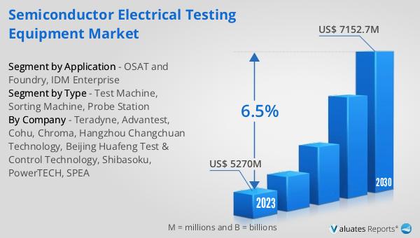
In the realm of technology, the Global Semiconductor Electrical Testing Equipment Market stands as a pivotal sector, ensuring the reliability and functionality of semiconductor devices before they are deployed in various applications. This market encompasses a broad array of equipment designed to test the electrical properties of semiconductors, a critical step in the manufacturing process. As semiconductors form the backbone of modern electronics, from smartphones to sophisticated computing systems, the demand for precise and efficient testing equipment has surged. The significance of this market lies in its role in maintaining the high standards of quality and performance expected in today's electronic products. By identifying defects and ensuring that semiconductor components meet the required specifications, electrical testing equipment helps in minimizing the risk of failures, thereby enhancing the overall reliability of electronic devices. This market's growth is propelled by the continuous advancements in semiconductor technology, including the development of smaller, faster, and more energy-efficient semiconductors, which necessitate more sophisticated testing solutions. As of 2023, the market's value was estimated at US$ 5270 million, with projections suggesting an increase to US$ 7152.7 million by 2030, marking a compound annual growth rate (CAGR) of 6.5%. This growth trajectory underscores the critical role of electrical testing equipment in the semiconductor industry's future, ensuring that as semiconductors become increasingly integral to technological progress, the tools used to test them evolve in tandem.

Semiconductor Electrical Testing Equipment Market

Test Machine, Sorting Machine, Probe Station in the Global Semiconductor Electrical Testing Equipment Market:

Diving deeper into the Global Semiconductor Electrical Testing Equipment Market, we find it segmented into various types of equipment, each serving a unique function in the semiconductor manufacturing process. Test machines, sorting machines, and probe stations represent the core categories of this market, each playing a crucial role in ensuring the quality and performance of semiconductor devices. Test machines are sophisticated devices that assess the electrical functionality of semiconductors under various conditions to ensure they meet the required performance standards. These machines are capable of conducting a wide range of tests, from basic electrical checks to complex functionality assessments, making them indispensable in the semiconductor manufacturing process. Sorting machines, on the other hand, are used to categorize semiconductors based on their performance characteristics. This process is vital for identifying and segregating components that meet the stringent quality standards from those that do not, thereby ensuring that only the highest quality semiconductors proceed to the next stages of production. Probe stations play a critical role in the early stages of semiconductor manufacturing. These devices are used to test the electrical properties of semiconductor wafers, identifying defects at an early stage and thus preventing the progression of faulty components through the manufacturing process. Together, these three types of equipment form the backbone of the Global Semiconductor Electrical Testing Equipment Market, each contributing to the meticulous process of semiconductor testing and quality assurance. Their combined use ensures that semiconductor devices are reliable, efficient, and capable of meeting the demands of various applications, from consumer electronics to industrial systems.

OSAT and Foundry, IDM Enterprise in the Global Semiconductor Electrical Testing Equipment Market:

The Global Semiconductor Electrical Testing Equipment Market finds its applications spread across various sectors, notably in Outsourced Semiconductor Assembly and Test (OSAT) services and Foundries, as well as Integrated Device Manufacturers (IDM) enterprises. In the OSAT and Foundry segment, electrical testing equipment plays a pivotal role in ensuring that semiconductors are assembled and tested to meet the highest standards of quality and performance. These services are crucial for companies that do not have their own semiconductor manufacturing facilities, relying instead on specialized providers to handle the assembly, testing, and packaging of their semiconductor devices. The use of advanced testing equipment in these settings helps in identifying potential defects and ensuring that only components that meet strict specifications are delivered to clients. This is particularly important in an industry where the functionality and reliability of semiconductor devices can significantly impact the final product's performance and consumer satisfaction. On the other hand, IDM enterprises, which control the entire semiconductor manufacturing process from design to assembly, also rely heavily on electrical testing equipment. In these companies, testing is an integral part of the production process, ensuring that every semiconductor device produced meets the company's stringent quality and performance criteria. The use of sophisticated testing equipment allows IDMs to maintain tight control over the quality of their products, thereby enhancing their competitiveness in the market. In both OSAT and Foundry services and IDM enterprises, the Global Semiconductor Electrical Testing Equipment Market is essential for maintaining the high standards of quality and reliability that are critical to the success of the semiconductor industry.

Global Semiconductor Electrical Testing Equipment Market Outlook:

The outlook for the Global Semiconductor Electrical Testing Equipment Market is notably positive, with its valuation in 2023 standing at US$ 5270 million and an expected rise to US$ 7152.7 million by 2030. This growth trajectory, marked by a compound annual growth rate (CAGR) of 6.5% during the forecast period from 2024 to 2030, highlights the robust demand and ongoing expansion within this sector. The market's growth is not confined to a single region; North America, Europe, and Japan collectively account for a significant portion of the market, holding a combined share of 23%. This widespread geographical distribution underscores the global reliance on semiconductor electrical testing equipment, reflecting the universal need for high-quality semiconductor devices across various industries. As semiconductors continue to play a crucial role in the advancement of technology, from consumer electronics to automotive and industrial applications, the demand for precise and efficient testing equipment is expected to remain strong. This market's growth is indicative of the increasing complexity and sophistication of semiconductor devices, necessitating advanced testing solutions to ensure their reliability and performance. The positive outlook for the Global Semiconductor Electrical Testing Equipment Market is a testament to the critical role it plays in the broader semiconductor industry, supporting the development and production of high-quality semiconductor components that are essential for the technological progress.


Report Metric Details
Report Name Semiconductor Electrical Testing Equipment Market
Accounted market size in 2023 US$ 5270 million
Forecasted market size in 2030 US$ 7152.7 million
CAGR 6.5%
Base Year 2023
Forecasted years 2024 - 2030
Segment by Type
  • Test Machine
  • Sorting Machine
  • Probe Station
Segment by Application
  • OSAT and Foundry
  • IDM Enterprise
Production by Region
  • North America
  • Europe
  • China
  • Japan
  • Southeast Asia
Consumption by Region
  • North America (United States, Canada)
  • Europe (Germany, France, UK, Italy, Russia)
  • Asia-Pacific (China, Japan, South Korea, Taiwan)
  • Southeast Asia (India)
  • Latin America (Mexico, Brazil)
By Company Teradyne, Advantest, Cohu, Chroma, Hangzhou Changchuan Technology, Beijing Huafeng Test & Control Technology, Shibasoku, PowerTECH, SPEA
Forecast units USD million in value
Report coverage Revenue and volume forecast, company share, competitive landscape, growth factors and trends

Global Wafer CMP Retainer Rings Market Research Report 2024

What is Global Wafer CMP Retainer Rings Market?

The Global Wafer CMP (Chemical Mechanical Planarization) Retainer Rings Market is a specialized segment within the semiconductor manufacturing industry, focusing on the production and distribution of retainer rings used in CMP processes. These rings play a crucial role in holding and securing the wafers in place during the planarization phase, which is essential for ensuring the flatness and uniformity of the wafer surface. The CMP process is a critical step in semiconductor fabrication, where it helps in smoothing surfaces and removing excess materials. The market for these retainer rings is driven by the demand for more efficient and advanced semiconductor devices, as the global electronics industry continues to evolve towards smaller, faster, and more complex components. With the semiconductor industry's growth, the need for high-quality CMP retainer rings has surged, making this market a key area of focus for manufacturers and suppliers aiming to meet the stringent requirements of wafer planarization.

Wafer CMP Retainer Rings Market

Polyphenylene Sulfide (PPS), Polyetheretherketone (PEEK), Polyethylene Terephthalate (PET), Others in the Global Wafer CMP Retainer Rings Market:

Diving into the materials used in the Global Wafer CMP Retainer Rings Market, we find a diverse range of high-performance polymers such as Polyphenylene Sulfide (PPS), Polyetheretherketone (PEEK), Polyethylene Terephthalate (PET), and others. Each of these materials offers unique properties that make them suitable for different aspects of CMP retainer ring production. PPS is known for its excellent chemical resistance and dimensional stability, which is crucial for maintaining the integrity of the wafer during the CMP process. PEEK, on the other hand, stands out for its high temperature resistance and mechanical strength, ensuring the retainer rings can withstand the rigorous conditions of CMP without deforming or failing. PET is valued for its good wear resistance and low friction, minimizing the risk of damaging the wafer surface during planarization. Other materials in the market also contribute specific benefits, such as enhanced durability or cost-effectiveness, allowing manufacturers to tailor their CMP retainer rings to meet the precise needs of semiconductor producers. The choice of material impacts not only the performance of the retainer rings but also the overall efficiency and reliability of the CMP process, making material selection a key strategic decision in this market.

300 mm Wafer, 200 mm Wafer, Others in the Global Wafer CMP Retainer Rings Market:

The usage of Global Wafer CMP Retainer Rings spans across various wafer sizes, including 300 mm, 200 mm, and others, catering to a wide range of semiconductor manufacturing needs. In the 300 mm wafer segment, the demand for CMP retainer rings is particularly high due to the larger surface area that requires planarization, making the process more challenging and the role of the retainer rings more critical. These rings ensure uniform application of pressure and prevent slippage, contributing to the high-quality finish required for advanced semiconductor devices. For the 200 mm wafer segment, although the wafers are smaller, the precision and reliability requirements remain stringent, necessitating the use of high-quality retainer rings that can deliver consistent performance. The "others" category includes emerging and specialized wafer sizes that cater to specific applications or newer technologies, where the CMP process and, consequently, the retainer rings must adapt to unique specifications and challenges. Across all these areas, the Global Wafer CMP Retainer Rings Market plays a vital role in enabling the production of semiconductors with the required surface flatness and smoothness, directly impacting the efficiency and performance of electronic devices.

Global Wafer CMP Retainer Rings Market Outlook:

The market outlook for the Global Wafer CMP Retainer Rings presents a promising growth trajectory, with the market's value estimated at US$ 108.9 million in 2023, and projections suggest it will ascend to US$ 144.6 million by 2030, marking a Compound Annual Growth Rate (CAGR) of 6.5% throughout the forecast period from 2024 to 2030. Despite a 2.0 percent decline in the Asia Pacific, the largest region, other areas have shown significant growth. The Americas, for instance, reported sales amounting to US$142.1 billion, reflecting a 17.0% increase on a year-on-year basis. Europe followed suit with sales reaching US$53.8 billion, up by 12.6% year-on-year, while Japan also saw a notable rise in sales to US$48.1 billion, marking a 10.0% increase from the previous year. However, the Asia-Pacific region, despite being the largest market, experienced a slight downturn with sales totaling US$336.2 billion, a 2.0% decrease year-on-year. This mixed performance across different regions highlights the dynamic nature of the Global Wafer CMP Retainer Rings Market, influenced by various factors including technological advancements, regional semiconductor manufacturing capacities, and global economic conditions.


Report Metric Details
Report Name Wafer CMP Retainer Rings Market
Accounted market size in 2023 US$ 108.9 million
Forecasted market size in 2030 US$ 144.6 million
CAGR 6.5%
Base Year 2023
Forecasted years 2024 - 2030
Segment by Type
  • Polyphenylene Sulfide (PPS)
  • Polyetheretherketone (PEEK)
  • Polyethylene Terephthalate (PET)
  • Others
Segment by Application
  • 300 mm Wafer
  • 200 mm Wafer
  • Others
Production by Region
  • North America
  • Europe
  • China
  • Japan
  • Taiwan
Consumption by Region
  • North America (United States, Canada)
  • Europe (Germany, France, UK, Italy, Russia)
  • Asia-Pacific (China, Japan, South Korea, Taiwan)
  • Southeast Asia (India)
  • Latin America (Mexico, Brazil)
By Company Akashi, Ensigner, Mitsubishi Chemical Advanced Materials, SPM Technology, SemPlastic, LLC, Victrex, Willbe S&T, TAK Materials Corporation, UIS Technologies, Calitech
Forecast units USD million in value
Report coverage Revenue and volume forecast, company share, competitive landscape, growth factors and trends

Global Wafer Used Etching Equipment Market Research Report 2024

What is Global Wafer Used Etching Equipment Market?

The Global Wafer Used Etching Equipment Market encompasses a specialized segment within the semiconductor manufacturing industry, focusing on the tools and technologies used to etch or remove layers from semiconductor wafers. This process is crucial in the fabrication of integrated circuits and microelectronic devices, where precision and control are paramount. Etching equipment plays a vital role in defining the microstructures that form the electrical circuits on a chip, enabling the production of smaller, faster, and more efficient electronic devices. As of 2023, the market for such equipment has been valued at US$ 22,660 million, reflecting the growing demand for advanced semiconductor components across various technology sectors. With projections suggesting a rise to US$ 29,860 million by 2030, the market is expected to experience a compound annual growth rate (CAGR) of 6.3%. This growth trajectory is underpinned by technological advancements, expanding applications in consumer electronics, automotive, and industrial automation, and the continuous push for miniaturization and performance enhancement of electronic devices. The market's dynamics are influenced by research and development activities, manufacturing capabilities, and the geographical distribution of key players, with North America, Europe, and Japan collectively holding a significant market share of 23%. This sector's evolution is closely tied to global technological trends and the semiconductor industry's cyclical nature, making it a critical area for investment and innovation.

Wafer Used Etching Equipment Market

Dry Etch Equipment, Wet Etch Equipment in the Global Wafer Used Etching Equipment Market:

In the realm of the Global Wafer Used Etching Equipment Market, two primary technologies stand out: Dry Etch Equipment and Wet Etch Equipment. Dry etching refers to the process of removing material from the semiconductor wafer using gases or plasmas to react with the material being etched away. This method is highly favored for its precision, ability to create complex patterns, and compatibility with the manufacturing of modern, densely packed integrated circuits. Dry etching equipment is crucial for applications requiring fine control over the etching process, such as in the creation of 3D structures and the etching of advanced materials. On the other hand, Wet etching involves the use of liquid chemicals or etchants to remove material from the wafer. This technique is characterized by its simplicity, cost-effectiveness, and high throughput, making it suitable for applications where less precision is required or when etching large areas. Despite the shift towards dry etching in many advanced semiconductor processes, wet etching remains relevant for certain steps in the manufacturing process, particularly in the cleaning and preparation of wafers. Both technologies are integral to the semiconductor manufacturing industry, each serving distinct roles that cater to the diverse needs of chip fabrication. The choice between dry and wet etching depends on various factors, including the material to be etched, the desired etch rate, the level of precision required, and cost considerations. As the Global Wafer Used Etching Equipment Market continues to evolve, the development and refinement of both dry and wet etching technologies remain critical for meeting the increasingly stringent requirements of semiconductor device fabrication.

IDM, Foundry in the Global Wafer Used Etching Equipment Market:

The Global Wafer Used Etching Equipment Market finds its applications significantly segmented into Integrated Device Manufacturers (IDM) and Foundries, each playing a crucial role in the semiconductor manufacturing ecosystem. IDMs are companies that design, manufacture, and sell semiconductor products, controlling the entire production process from design to device fabrication. In this context, etching equipment is used to sculpt and shape semiconductor materials into the intricate patterns required for integrated circuits, making it a cornerstone of IDM operations. The precision and capability of etching equipment directly impact the performance, yield, and cost-effectiveness of semiconductor devices, highlighting its importance in maintaining competitive advantage and technological leadership. Foundries, on the other hand, are specialized facilities that manufacture semiconductor devices on behalf of other companies. These entities rely heavily on advanced etching equipment to meet the diverse and complex requirements of their clients, ensuring that chips are produced to exact specifications with high reliability and efficiency. The use of cutting-edge etching technologies in foundries enables the production of smaller, more powerful semiconductor devices, catering to the ever-increasing demands of the technology sector. Both IDMs and foundries are integral to the semiconductor industry's supply chain, with etching equipment serving as a critical tool in the fabrication of electronic devices. As the market for semiconductor devices continues to expand, driven by advancements in technology and increasing electronic content in various industries, the role of etching equipment in IDMs and foundries is set to become even more pivotal.

Global Wafer Used Etching Equipment Market Outlook:

In 2023, the market for Wafer Used Etching Equipment was estimated at a value of US$ 22,660 million, showcasing the significant demand within the semiconductor manufacturing sector for high-precision etching tools. This market is on a trajectory of growth, expected to ascend to a valuation of US$ 29,860 million by the year 2030. This progression represents a compound annual growth rate (CAGR) of 6.3% over the forecast period stretching from 2024 to 2030. Such growth is indicative of the increasing reliance on sophisticated semiconductor devices across a multitude of industries, driving the need for advanced etching equipment capable of producing intricate microelectronic components. The combined market share held by North America, Europe, and Japan, which stands at 23%, underscores the global nature of this market, highlighting the widespread adoption and integration of etching technologies in key technological hubs around the world. This outlook reflects not only the current state of the market but also its potential for expansion as innovations in semiconductor technology continue to push the boundaries of what is possible in electronic device fabrication.


Report Metric Details
Report Name Wafer Used Etching Equipment Market
Accounted market size in 2023 US$ 22660 million
Forecasted market size in 2030 US$ 29860 million
CAGR 6.3%
Base Year 2023
Forecasted years 2024 - 2030
Segment by Type
  • Dry Etch Equipment
  • Wet Etch Equipment
Segment by Application
  • IDM
  • Foundry
Production by Region
  • North America
  • Europe
  • China
  • Japan
Consumption by Region
  • North America (United States, Canada)
  • Europe (Germany, France, UK, Italy, Russia)
  • Asia-Pacific (China, Japan, South Korea, Taiwan)
  • Southeast Asia (India)
  • Latin America (Mexico, Brazil)
By Company Lam Research, Tokyo Electron Limited, Applied Materials, Hitachi High-Tech, SEMES, AMEC, NAURA, SPTS Technologies (KLA), Oxford Instruments, ULVAC, Plasma-Therm
Forecast units USD million in value
Report coverage Revenue and volume forecast, company share, competitive landscape, growth factors and trends

Global Wafer Used CVD Equipment Market Research Report 2024

What is Global Wafer Used CVD Equipment Market?

The Global Wafer Used CVD (Chemical Vapor Deposition) Equipment Market is a specialized sector within the semiconductor manufacturing industry, focusing on the equipment used for the CVD process. This process is crucial for creating high-quality, high-performance solid materials, typically wafers, used in the production of semiconductors. The equipment plays a pivotal role in depositing various types of materials onto the semiconductor wafers through a chemical vapor deposition method. This involves a chemical reaction occurring between the gaseous phase and the wafer surface, leading to the deposition of the desired material. The market for such equipment has seen significant growth due to the increasing demand for semiconductors in various applications, including electronics, automotive, and telecommunications. The value of this market was estimated at US$ 9893.5 million in 2023 and is projected to expand to US$ 13190 million by 2030, with a compound annual growth rate (CAGR) of 6.1% during the forecast period from 2024 to 2030. This growth is attributed to technological advancements, the rising demand for electronic devices, and the expansion of semiconductor manufacturing capabilities across the globe. North America, Europe, and Japan collectively hold a significant portion of the market share, indicating their influential role in the global landscape of wafer used CVD equipment.

Wafer Used CVD Equipment Market

PECVD, LPCVD, ALD, Others in the Global Wafer Used CVD Equipment Market:

In the realm of the Global Wafer Used CVD Equipment Market, technologies such as PECVD (Plasma Enhanced Chemical Vapor Deposition), LPCVD (Low-Pressure Chemical Vapor Deposition), ALD (Atomic Layer Deposition), and others play critical roles. PECVD is widely utilized for depositing thin films from a gas state to a solid state on a substrate. This method is particularly beneficial for applications requiring lower temperature processes, making it ideal for depositing films on temperature-sensitive substrates. LPCVD, on the other hand, is favored for its uniformity and purity of the deposited layers, crucial for manufacturing semiconductors where consistency is key. ALD is renowned for its precision and ability to deposit ultra-thin films, allowing for the production of nanoscale devices with high aspect ratios. Each of these technologies caters to specific requirements within the semiconductor manufacturing process, highlighting the diversity and complexity of the market. The choice of CVD technology impacts the quality, efficiency, and application of the final semiconductor products, underscoring the importance of these methods in advancing the semiconductor industry. The continuous evolution and innovation within these technologies reflect the dynamic nature of the Global Wafer Used CVD Equipment Market, driving its expansion and adaptation to meet the ever-changing demands of semiconductor manufacturing.

IDM, Foundry in the Global Wafer Used CVD Equipment Market:

The usage of Global Wafer Used CVD Equipment in IDM (Integrated Device Manufacturers) and Foundry sectors underscores the pivotal role of CVD technologies in the semiconductor manufacturing process. In the IDM sector, where companies control the entire production process from design to manufacturing, CVD equipment is essential for ensuring the high quality and performance of semiconductor devices. These manufacturers rely on advanced CVD technologies to deposit various materials onto semiconductor wafers, enabling the production of complex and miniaturized electronic components. The precision and efficiency offered by CVD equipment are critical for IDMs to maintain competitiveness and meet the stringent requirements of modern electronic devices. Similarly, in the Foundry sector, which specializes in manufacturing semiconductors for design firms without their fabrication facilities, CVD equipment plays a crucial role. Foundries must offer cutting-edge manufacturing capabilities, including sophisticated CVD processes, to attract and retain clients seeking to produce innovative semiconductor products. The ability to provide advanced CVD technologies is a key differentiator for foundries, enabling them to support the production of next-generation semiconductors with enhanced features and performance. The demand for CVD equipment in both IDM and Foundry sectors is driven by the ongoing miniaturization of electronic devices, the complexity of semiconductor manufacturing processes, and the need for high-quality, reliable semiconductor components.

Global Wafer Used CVD Equipment Market Outlook:

The market outlook for Global Wafer Used CVD Equipment presents a promising future, with the market's value standing at US$ 9893.5 million in 2023 and expected to ascend to US$ 13190 million by 2030. This growth trajectory, marked by a CAGR of 6.1% during the forecast period from 2024 to 2030, underscores the robust demand and technological advancements propelling the sector forward. The combined market share of North America, Europe, and Japan, which accounts for 23%, highlights the significant contribution of these regions to the global market. This growth is reflective of the increasing reliance on semiconductors across various industries, including but not limited to electronics, automotive, and telecommunications, which in turn fuels the demand for CVD equipment. The expansion of semiconductor manufacturing capabilities, coupled with the technological evolution in CVD processes, plays a crucial role in meeting the burgeoning demand for high-quality semiconductors. The market's growth prospects are buoyed by the continuous innovation within the sector, aiming to address the complex requirements of modern semiconductor production and ensuring the market's resilience and relevance in the face of evolving technological landscapes.


Report Metric Details
Report Name Wafer Used CVD Equipment Market
Accounted market size in 2023 US$ 9893.5 million
Forecasted market size in 2030 US$ 13190 million
CAGR 6.1%
Base Year 2023
Forecasted years 2024 - 2030
Segment by Type
  • PECVD
  • LPCVD
  • ALD
  • Others
Segment by Application
  • IDM
  • Foundry
Production by Region
  • North America
  • Europe
  • China
  • Japan
  • Korea
Consumption by Region
  • North America (United States, Canada)
  • Europe (Germany, France, UK, Italy, Russia)
  • Asia-Pacific (China, Japan, South Korea, Taiwan)
  • Southeast Asia (India)
  • Latin America (Mexico, Brazil)
By Company Applied Materials, Lam Research, Tokyo Electron, ASM International, Kokusai Electric, Wonik IPS, Eugene Technology, Jusung Engineering, TES, SPTS Technologies (KLA), Veeco, CVD Equipment, Piotech, NAURA Technology
Forecast units USD million in value
Report coverage Revenue and volume forecast, company share, competitive landscape, growth factors and trends

Global Perfluoroelastomer (FFKM) Seals and Parts for Semiconductor Market Research Report 2024

What is Global Perfluoroelastomer (FFKM) Seals and Parts for Semiconductor Market?

In 2023, the market for Perfluoroelastomer (FFKM) Seals and Parts specifically designed for the semiconductor industry was estimated to be worth $206 million. This niche yet crucial market is expected to grow steadily, reaching a valuation of $275.8 million by the year 2030. This growth trajectory represents a compound annual growth rate (CAGR) of 6.1% over the forecast period from 2024 to 2030. It's noteworthy that the market is highly concentrated, with the top three companies commanding more than 85% of the overall market share. This concentration highlights the specialized nature of the FFKM seals and parts production, underscoring the significant barriers to entry for new competitors and the high level of expertise required to manufacture these essential components for the semiconductor industry. The robust growth forecasted for this market is indicative of the increasing demand for semiconductors and the critical role that high-quality seals and parts play in ensuring the reliability and performance of semiconductor manufacturing equipment.

Perfluoroelastomer (FFKM) Seals and Parts for Semiconductor Market

O-Ring, Gasket, Others in the Global Perfluoroelastomer (FFKM) Seals and Parts for Semiconductor Market:

English: #Perfluoroelastomer #SemiconductorMarket #FFKMSeals #MarketGrowth #IndustryForecast #HighPerformanceSeals #SemiconductorManufacturing #MarketLeaders #TechnologyTrends #GlobalMarket

Wafer Suppliers, Semiconductor Equipment OEMs in the Global Perfluoroelastomer (FFKM) Seals and Parts for Semiconductor Market:

Japanese: #フッ素エラストマー #半導体市場 #FFKMシール #市場成長 #業界予測 #高性能シール #半導体製造 #市場リーダー #技術トレンド #グローバル市場

Global Perfluoroelastomer (FFKM) Seals and Parts for Semiconductor Market Outlook:

Korean: #퍼플루오로엘라스토머 #반도체시장 #FFKM씰 #시장성장 #산업예측 #고성능씰 #반도체제조 #시장리더 #기술트렌드 #글로벌시장


Report Metric Details
Report Name Perfluoroelastomer (FFKM) Seals and Parts for Semiconductor Market
Accounted market size in 2023 US$ 206 million
Forecasted market size in 2030 US$ 275.8 million
CAGR 6.1%
Base Year 2023
Forecasted years 2024 - 2030
Segment by Type
  • O-Ring
  • Gasket
  • Others
Segment by Application
  • Wafer Suppliers
  • Semiconductor Equipment OEMs
By Region
  • North America (United States, Canada)
  • Europe (Germany, France, UK, Italy, Russia) Rest of Europe
  • Nordic Countries
  • Asia-Pacific (China, Japan, South Korea)
  • Southeast Asia (India, Australia)
  • Rest of Asia
  • Latin America (Mexico, Brazil)
  • Rest of Latin America
  • Middle East & Africa (Turkey, Saudi Arabia, UAE, Rest of MEA)
By Company DuPont, 3M, Solvay, Daikin, Asahi Glass, Trelleborg, Greene Tweed
Forecast units USD million in value
Report coverage Revenue and volume forecast, company share, competitive landscape, growth factors and trends

Global Wide Bandgap Power (WBG) Semiconductor Power Devices and Modules Market Research Report 2024

What is Global Wide Bandgap Power (WBG) Semiconductor Power Devices and Modules Market?

The Global Wide Bandgap Power (WBG) Semiconductor Power Devices and Modules Market is a cutting-edge sector that's revolutionizing how we manage and utilize power in various electronic devices and systems. At its core, this market focuses on the development and application of semiconductor materials that have a wider bandgap compared to traditional silicon-based semiconductors. These materials, such as silicon carbide (SiC) and gallium nitride (GaN), allow for the creation of power devices and modules that operate more efficiently, at higher temperatures, and with greater power density. This means they can switch on and off much faster, waste less energy, and handle higher voltages than their silicon counterparts. The significance of these advancements cannot be overstated, as they pave the way for more efficient, compact, and reliable power systems across a wide range of industries, including renewable energy, automotive, and consumer electronics, to name a few. The push towards electrification and sustainable energy solutions has only heightened the demand for WBG semiconductor power devices and modules, positioning this market as a pivotal player in the global transition towards cleaner and more efficient energy use.

Wide Bandgap Power (WBG) Semiconductor Power Devices and Modules Market

Power SiC Devices and Modules, Power GaN Devices and Modules in the Global Wide Bandgap Power (WBG) Semiconductor Power Devices and Modules Market:

Diving into the specifics, the Global Wide Bandgap Power (WBG) Semiconductor Power Devices and Modules Market is primarily segmented into Power SiC Devices and Modules, and Power GaN Devices and Modules. These two categories represent the forefront of semiconductor technology, offering remarkable benefits over traditional silicon-based solutions. Power SiC Devices and Modules, for instance, are renowned for their exceptional efficiency and high-temperature performance, making them ideal for high-power applications such as electric vehicles (EVs), industrial motor drives, and power grid infrastructure. Their ability to operate at higher temperatures significantly reduces cooling requirements, thereby shrinking the size and cost of the overall system. On the other hand, Power GaN Devices and Modules stand out for their high-frequency operation capabilities, which translate into smaller, lighter, and more efficient power supplies and converters. This makes them particularly suited for fast-charging EV infrastructure, renewable energy systems, and compact consumer electronics. Both SiC and GaN technologies are driving the innovation in power electronics, enabling more efficient energy conversion, reducing energy loss, and contributing to the development of smaller, lighter, and more energy-efficient products. As the demand for cleaner energy and more efficient electronic devices continues to grow, the role of Power SiC and GaN Devices and Modules within the Global Wide Bandgap Power Semiconductor Power Devices and Modules Market is becoming increasingly vital, marking a significant shift away from traditional power semiconductor technologies.

Electric Vehicle, Photovoltaic and Energy Storage Systems, Electric Vehicle Charging Infrastructure, PFC Power Supply, Motor Drive, UPS, Others in the Global Wide Bandgap Power (WBG) Semiconductor Power Devices and Modules Market:

The usage of Global Wide Bandgap Power (WBG) Semiconductor Power Devices and Modules spans across a diverse range of applications, each benefiting from the enhanced efficiency, reliability, and performance these technologies offer. In the realm of Electric Vehicles (EVs), WBG semiconductors are instrumental in improving the range and efficiency of EVs through more efficient power conversion and reduced energy losses, which is crucial for accelerating the adoption of electric mobility. Similarly, in Photovoltaic (PV) and Energy Storage Systems, these devices enable more efficient conversion of solar energy into electricity and improve the efficiency and lifespan of energy storage systems, thereby supporting the growth of renewable energy solutions. The Electric Vehicle Charging Infrastructure also benefits from WBG technologies, where their high efficiency and fast switching capabilities are essential for developing fast-charging stations that reduce waiting times for EV users. In Power Factor Correction (PFC) Power Supplies and Motor Drives, WBG devices ensure more efficient operation, leading to energy savings and reduced operational costs in industrial and consumer applications. Uninterruptible Power Supplies (UPS) systems equipped with WBG semiconductors can achieve higher efficiency and reliability, ensuring the protection and continuous operation of critical systems and networks. The 'Others' category, which includes applications like RF and microwave devices, benefits from the high-frequency operation capabilities of GaN devices, opening up new possibilities in telecommunications and beyond. The widespread adoption of WBG semiconductor power devices and modules across these areas is a testament to their transformative potential, driving efficiency, and innovation in a world increasingly reliant on electronic systems and renewable energy sources.

Global Wide Bandgap Power (WBG) Semiconductor Power Devices and Modules Market Outlook:

The market outlook for the global semiconductor industry presents a promising trajectory, with the sector's valuation estimated at US$ 579 billion in 2022, and projections indicating a growth to US$ 790 billion by 2029. This growth, expected to occur at a compound annual growth rate (CAGR) of 6% during the forecast period, underscores the robust demand and ongoing innovation within the semiconductor space. Such expansion is reflective of the increasing reliance on semiconductor technologies across a multitude of industries, from automotive to consumer electronics and renewable energy systems. The surge in demand is particularly fueled by the advancements in technologies such as Wide Bandgap (WBG) semiconductors, which are pivotal in driving efficiency, performance, and sustainability in electronic devices and systems. This market growth not only highlights the critical role semiconductors play in the modern economy but also points to the sector's potential in facilitating the global transition towards more energy-efficient and high-performance electronic solutions. As industries continue to evolve and integrate more sophisticated electronic components, the semiconductor market's growth trajectory is poised to remain on an upward path, reflecting its indispensable role in powering the future of technology.


Report Metric Details
Report Name Wide Bandgap Power (WBG) Semiconductor Power Devices and Modules Market
Accounted market size in year US$ 579 billion
Forecasted market size in 2029 US$ 790 billion
CAGR 6%
Base Year year
Forecasted years 2024 - 2029
Segment by Type
  • Power SiC Devices and Modules
  • Power GaN Devices and Modules
Segment by Application
  • Electric Vehicle
  • Photovoltaic and Energy Storage Systems
  • Electric Vehicle Charging Infrastructure
  • PFC Power Supply
  • Motor Drive
  • UPS
  • Others
By Region
  • North America (United States, Canada)
  • Europe (Germany, France, UK, Italy, Russia) Rest of Europe
  • Nordic Countries
  • Asia-Pacific (China, Japan, South Korea)
  • Southeast Asia (India, Australia)
  • Rest of Asia
  • Latin America (Mexico, Brazil)
  • Rest of Latin America
  • Middle East & Africa (Turkey, Saudi Arabia, UAE, Rest of MEA)
By Company Wolfspped (Cree), Infineon Technologies, ROHM Semiconductor, STMicroelectronics, Onsemi, Mitsubishi Electric, Littelfuse, Microchip Technology, GeneSiC Semiconductor, Transphorm, GaN Systems, Navitas Semiconductor, Efficient Power Conversion (EPC)
Forecast units USD million in value
Report coverage Revenue and volume forecast, company share, competitive landscape, growth factors and trends

Global Semiconductor Wafers Used CMP Pad Market Research Report 2024

What is Global Semiconductor Wafers Used CMP Pad Market?

The Global Semiconductor Wafers Used CMP Pad Market is a niche yet crucial segment within the semiconductor industry, focusing on the production and sale of CMP (Chemical Mechanical Planarization) pads. These pads are essential for the manufacturing process of semiconductor wafers, as they help in smoothing and leveling the wafer's surface through a combination of chemical and mechanical processes. The market's significance stems from the ever-increasing demand for semiconductor devices across various sectors, including electronics, automotive, and telecommunications, which in turn drives the need for high-quality CMP pads. As of 2023, the market was valued at US$ 1071.7 million, showcasing the substantial investment and development within this sector. With technological advancements and the growing complexity of semiconductor devices, the CMP pad market is expected to expand further, reaching an estimated value of US$ 1412.2 million by 2030. This growth trajectory, marked by a compound annual growth rate (CAGR) of 7.1% during the forecast period from 2024 to 2030, highlights the market's dynamic nature and its critical role in supporting the broader semiconductor manufacturing industry.

Semiconductor Wafers Used CMP Pad Market

Hard CMP Pads, Soft CMP Pads in the Global Semiconductor Wafers Used CMP Pad Market:

In the realm of the Global Semiconductor Wafers Used CMP Pad Market, CMP pads are categorized mainly into two types: Hard CMP Pads and Soft CMP Pads, each serving distinct purposes based on their material composition and intended application. Hard CMP pads are typically made from materials that offer higher rigidity and are used in the initial stages of the CMP process, where more substantial material removal is required. These pads are crucial for efficiently reducing surface topography and preparing the wafer for subsequent processing steps. On the other hand, Soft CMP Pads are designed with more pliable materials, making them ideal for the final polishing phases where a finer, more delicate touch is needed to achieve the desired surface smoothness and defect removal. The choice between hard and soft CMP pads depends on several factors, including the type of material being polished, the specific layer of the semiconductor device being processed, and the desired outcome in terms of surface finish and planarity. The development and optimization of these pads are driven by the continuous evolution of semiconductor devices, which demand higher precision and reliability from the CMP process. As such, manufacturers in the Global Semiconductor Wafers Used CMP Pad Market invest heavily in research and development to enhance the performance and efficiency of both hard and soft CMP pads, catering to the intricate needs of semiconductor wafer processing.

300 mm Wafer, 200 mm Wafer, Others in the Global Semiconductor Wafers Used CMP Pad Market:

The usage of CMP pads in the Global Semiconductor Wafers Used CMP Pad Market is primarily segmented by the size of the semiconductor wafers they are designed to process, with 300 mm and 200 mm wafers being the most common, alongside other sizes. The 300 mm wafer segment represents the forefront of semiconductor manufacturing, offering economies of scale and higher throughput for manufacturers, thus requiring CMP pads that can accommodate their larger size and the increased complexity of devices they house. These pads are engineered to deliver uniform polishing across the wafer's broader surface area, ensuring high-quality device fabrication. The 200 mm wafer segment, while older, remains relevant in the production of certain types of semiconductor devices. CMP pads designed for 200 mm wafers are tailored to meet the specific requirements of these manufacturing processes, balancing cost-effectiveness with the need for precision and reliability. The "Others" category encompasses CMP pads for wafers of different sizes, catering to specialized applications or legacy manufacturing processes that do not conform to the standard 300 mm or 200 mm formats. This segmentation by wafer size highlights the versatility and adaptability of the CMP pad market to meet the diverse needs of the semiconductor industry, ensuring that manufacturers have access to the right tools for every step of the wafer processing workflow.

Global Semiconductor Wafers Used CMP Pad Market Outlook:

The market outlook for Global Semiconductor Wafers Used CMP Pad Market presents a promising future, with the sector's valuation at US$ 1071.7 million in 2023, and an expected growth to US$ 1412.2 million by the year 2030. This projection indicates a steady compound annual growth rate (CAGR) of 7.1% throughout the period spanning from 2024 to 2030. Such growth is indicative of the increasing reliance on semiconductor devices across various industries, driving the demand for CMP pads which are essential in the production of these devices. The CMP pad market's expansion is further fueled by technological advancements and the scaling of semiconductor manufacturing processes, necessitating more efficient and effective CMP pads. This upward trend underscores the critical role CMP pads play in the semiconductor manufacturing ecosystem, ensuring the production of high-quality wafers necessary for the burgeoning demand for electronic devices, automotive components, and other technological innovations. The market's robust growth prospects highlight its importance and the opportunities it presents for stakeholders within the semiconductor manufacturing chain.


Report Metric Details
Report Name Semiconductor Wafers Used CMP Pad Market
Accounted market size in 2023 US$ 1071.7 million
Forecasted market size in 2030 US$ 1412.2 million
CAGR 7.1%
Base Year 2023
Forecasted years 2024 - 2030
Segment by Type
  • Hard CMP Pads
  • Soft CMP Pads
Segment by Application
  • 300 mm Wafer
  • 200 mm Wafer
  • Others
Production by Region
  • North America
  • Europe
  • China
  • Japan
  • Korea
  • Taiwan
Consumption by Region
  • North America (United States, Canada)
  • Europe (Germany, France, UK, Italy, Russia)
  • Asia-Pacific (China, Japan, South Korea, Taiwan)
  • Southeast Asia (India)
  • Latin America (Mexico, Brazil)
By Company DuPont, CMC Materials, FUJIBO, IVT Technologies, SKC, Hubei Dinglong, TWI Incorporated, 3M, FNS TECH, KPX
Forecast units USD million in value
Report coverage Revenue and volume forecast, company share, competitive landscape, growth factors and trends

Global Low-Temperature Electrolyte Additives Market Research Report 2025

What is Global Low-Temperature Electrolyte Additives Market? The Global Low-Temperature Electrolyte Additives Market is a specialized segme...