What is Global Semiconductor Wafers Used CMP Pad Market?
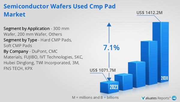
The Global Semiconductor Wafers Used CMP Pad Market is a niche yet crucial segment within the semiconductor industry, focusing on the production and sale of CMP (Chemical Mechanical Planarization) pads. These pads are essential for the manufacturing process of semiconductor wafers, as they help in smoothing and leveling the wafer's surface through a combination of chemical and mechanical processes. The market's significance stems from the ever-increasing demand for semiconductor devices across various sectors, including electronics, automotive, and telecommunications, which in turn drives the need for high-quality CMP pads. As of 2023, the market was valued at US$ 1071.7 million, showcasing the substantial investment and development within this sector. With technological advancements and the growing complexity of semiconductor devices, the CMP pad market is expected to expand further, reaching an estimated value of US$ 1412.2 million by 2030. This growth trajectory, marked by a compound annual growth rate (CAGR) of 7.1% during the forecast period from 2024 to 2030, highlights the market's dynamic nature and its critical role in supporting the broader semiconductor manufacturing industry.
Hard CMP Pads, Soft CMP Pads in the Global Semiconductor Wafers Used CMP Pad Market:
In the realm of the Global Semiconductor Wafers Used CMP Pad Market, CMP pads are categorized mainly into two types: Hard CMP Pads and Soft CMP Pads, each serving distinct purposes based on their material composition and intended application. Hard CMP pads are typically made from materials that offer higher rigidity and are used in the initial stages of the CMP process, where more substantial material removal is required. These pads are crucial for efficiently reducing surface topography and preparing the wafer for subsequent processing steps. On the other hand, Soft CMP Pads are designed with more pliable materials, making them ideal for the final polishing phases where a finer, more delicate touch is needed to achieve the desired surface smoothness and defect removal. The choice between hard and soft CMP pads depends on several factors, including the type of material being polished, the specific layer of the semiconductor device being processed, and the desired outcome in terms of surface finish and planarity. The development and optimization of these pads are driven by the continuous evolution of semiconductor devices, which demand higher precision and reliability from the CMP process. As such, manufacturers in the Global Semiconductor Wafers Used CMP Pad Market invest heavily in research and development to enhance the performance and efficiency of both hard and soft CMP pads, catering to the intricate needs of semiconductor wafer processing.
300 mm Wafer, 200 mm Wafer, Others in the Global Semiconductor Wafers Used CMP Pad Market:
The usage of CMP pads in the Global Semiconductor Wafers Used CMP Pad Market is primarily segmented by the size of the semiconductor wafers they are designed to process, with 300 mm and 200 mm wafers being the most common, alongside other sizes. The 300 mm wafer segment represents the forefront of semiconductor manufacturing, offering economies of scale and higher throughput for manufacturers, thus requiring CMP pads that can accommodate their larger size and the increased complexity of devices they house. These pads are engineered to deliver uniform polishing across the wafer's broader surface area, ensuring high-quality device fabrication. The 200 mm wafer segment, while older, remains relevant in the production of certain types of semiconductor devices. CMP pads designed for 200 mm wafers are tailored to meet the specific requirements of these manufacturing processes, balancing cost-effectiveness with the need for precision and reliability. The "Others" category encompasses CMP pads for wafers of different sizes, catering to specialized applications or legacy manufacturing processes that do not conform to the standard 300 mm or 200 mm formats. This segmentation by wafer size highlights the versatility and adaptability of the CMP pad market to meet the diverse needs of the semiconductor industry, ensuring that manufacturers have access to the right tools for every step of the wafer processing workflow.
Global Semiconductor Wafers Used CMP Pad Market Outlook:
The market outlook for Global Semiconductor Wafers Used CMP Pad Market presents a promising future, with the sector's valuation at US$ 1071.7 million in 2023, and an expected growth to US$ 1412.2 million by the year 2030. This projection indicates a steady compound annual growth rate (CAGR) of 7.1% throughout the period spanning from 2024 to 2030. Such growth is indicative of the increasing reliance on semiconductor devices across various industries, driving the demand for CMP pads which are essential in the production of these devices. The CMP pad market's expansion is further fueled by technological advancements and the scaling of semiconductor manufacturing processes, necessitating more efficient and effective CMP pads. This upward trend underscores the critical role CMP pads play in the semiconductor manufacturing ecosystem, ensuring the production of high-quality wafers necessary for the burgeoning demand for electronic devices, automotive components, and other technological innovations. The market's robust growth prospects highlight its importance and the opportunities it presents for stakeholders within the semiconductor manufacturing chain.
| Report Metric | Details |
| Report Name | Semiconductor Wafers Used CMP Pad Market |
| Accounted market size in 2023 | US$ 1071.7 million |
| Forecasted market size in 2030 | US$ 1412.2 million |
| CAGR | 7.1% |
| Base Year | 2023 |
| Forecasted years | 2024 - 2030 |
| Segment by Type |
|
| Segment by Application |
|
| Production by Region |
|
| Consumption by Region |
|
| By Company | DuPont, CMC Materials, FUJIBO, IVT Technologies, SKC, Hubei Dinglong, TWI Incorporated, 3M, FNS TECH, KPX |
| Forecast units | USD million in value |
| Report coverage | Revenue and volume forecast, company share, competitive landscape, growth factors and trends |


