What is Global GaAs Single Crystal Wafers Market?
The Global GaAs Single Crystal Wafers Market is a specialized segment within the semiconductor industry, focusing on the production and distribution of gallium arsenide (GaAs) single crystal wafers. These wafers are crucial components in the manufacturing of various electronic devices due to their superior electron mobility and ability to operate at high frequencies. GaAs wafers are primarily used in applications that require high efficiency and performance, such as radio frequency (RF) devices, light-emitting diodes (LEDs), vertical-cavity surface-emitting lasers (VCSELs), and photovoltaic (PV) cells. The market for these wafers is driven by the increasing demand for high-speed and high-frequency electronic devices, which are essential in modern communication systems, consumer electronics, and renewable energy solutions. As technology continues to advance, the need for more efficient and reliable semiconductor materials like GaAs is expected to grow, further propelling the market. The global GaAs single crystal wafers market is characterized by continuous research and development efforts aimed at improving wafer quality and reducing production costs, making it a dynamic and evolving sector within the broader semiconductor industry.
in the Global GaAs Single Crystal Wafers Market:
In the Global GaAs Single Crystal Wafers Market, various types of wafers are utilized by different customers based on their specific needs and applications. The primary types of GaAs wafers include semi-insulating and semi-conducting wafers. Semi-insulating GaAs wafers are predominantly used in RF and microwave applications due to their excellent electrical insulation properties, which minimize signal loss and interference. These wafers are essential in the production of high-frequency devices such as amplifiers, oscillators, and switches used in telecommunications and radar systems. On the other hand, semi-conducting GaAs wafers are used in optoelectronic applications, including LEDs and laser diodes, due to their ability to efficiently convert electrical energy into light. These wafers are integral in the manufacturing of devices that require high brightness and efficiency, such as display panels and optical communication systems. Additionally, GaAs wafers are available in different diameters, typically ranging from 2 inches to 6 inches, to accommodate various manufacturing processes and device specifications. The choice of wafer diameter depends on the production scale and the specific requirements of the end application. Larger wafers are preferred for mass production due to their ability to yield more devices per wafer, thereby reducing overall production costs. Furthermore, the surface orientation of GaAs wafers, such as (100) or (111), plays a crucial role in determining their suitability for specific applications. The (100) orientation is commonly used for electronic devices, while the (111) orientation is preferred for certain optoelectronic applications due to its favorable crystallographic properties. Customers in the GaAs single crystal wafers market also consider factors such as wafer thickness, doping concentration, and surface finish when selecting wafers for their applications. Thinner wafers are often used in applications where weight and space are critical, such as in portable electronic devices. Doping concentration, which refers to the amount of impurity atoms added to the wafer, is carefully controlled to achieve the desired electrical properties for specific applications. A smooth surface finish is essential for ensuring optimal device performance and reliability, as it reduces the likelihood of defects and improves the efficiency of subsequent manufacturing processes. Overall, the diverse types of GaAs single crystal wafers available in the market cater to a wide range of customer needs, enabling the production of high-performance electronic and optoelectronic devices across various industries.
RF, LED, VCSEL, PV in the Global GaAs Single Crystal Wafers Market:
The usage of Global GaAs Single Crystal Wafers Market in RF, LED, VCSEL, and PV applications highlights the versatility and importance of these wafers in modern technology. In RF applications, GaAs wafers are prized for their high electron mobility and ability to operate at high frequencies, making them ideal for use in RF amplifiers, switches, and oscillators. These devices are critical components in wireless communication systems, including mobile phones, satellite communications, and radar systems, where high-speed data transmission and signal integrity are paramount. The superior performance of GaAs-based RF devices compared to silicon-based counterparts makes them a preferred choice in applications that demand high efficiency and reliability. In the LED industry, GaAs wafers are used as substrates for the growth of gallium arsenide phosphide (GaAsP) and aluminum gallium arsenide (AlGaAs) layers, which are essential for producing high-brightness LEDs. These LEDs are widely used in display panels, automotive lighting, and general illumination due to their energy efficiency and long lifespan. The ability of GaAs wafers to support the growth of high-quality epitaxial layers ensures that the resulting LEDs exhibit excellent optical and electrical properties, making them suitable for a wide range of lighting applications. VCSELs, or vertical-cavity surface-emitting lasers, are another key application of GaAs single crystal wafers. These lasers are used in optical communication systems, data centers, and 3D sensing technologies due to their high-speed modulation capabilities and low power consumption. GaAs wafers provide an ideal substrate for the fabrication of VCSELs, enabling the production of devices with high performance and reliability. The use of GaAs-based VCSELs in applications such as facial recognition, gesture control, and LiDAR systems underscores the growing importance of these wafers in advanced sensing technologies. In the photovoltaic (PV) sector, GaAs wafers are used in the production of high-efficiency solar cells. GaAs-based solar cells offer superior performance compared to traditional silicon-based cells, particularly in terms of efficiency and temperature stability. These cells are often used in space applications, where their high efficiency and radiation resistance are critical for reliable power generation. The ability of GaAs wafers to support the growth of multi-junction solar cells, which consist of multiple layers of different semiconductor materials, further enhances their appeal in the PV market. These multi-junction cells can achieve significantly higher efficiencies than single-junction cells, making them ideal for use in concentrated photovoltaic systems and other high-performance solar applications. Overall, the diverse applications of GaAs single crystal wafers in RF, LED, VCSEL, and PV technologies underscore their critical role in enabling the development of advanced electronic and optoelectronic devices.
Global GaAs Single Crystal Wafers Market Outlook:
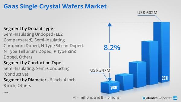
The global market for GaAs Single Crystal Wafers was valued at $347 million in 2024, with projections indicating a growth to $602 million by 2031. This represents a compound annual growth rate (CAGR) of 8.2% over the forecast period. This growth trajectory underscores the increasing demand for GaAs wafers across various high-tech industries. The rising adoption of GaAs wafers in RF applications, driven by the expanding telecommunications sector and the need for high-frequency devices, is a significant factor contributing to this market growth. Additionally, the growing use of GaAs wafers in LED and VCSEL applications, fueled by advancements in optoelectronic technologies and the increasing demand for energy-efficient lighting solutions, further propels the market. The photovoltaic sector also plays a crucial role in the market's expansion, as GaAs-based solar cells offer superior efficiency and performance compared to traditional silicon-based cells. The ability of GaAs wafers to support the development of high-performance electronic and optoelectronic devices makes them an indispensable component in modern technology. As industries continue to seek more efficient and reliable semiconductor materials, the demand for GaAs single crystal wafers is expected to grow, driving the market towards its projected size by 2031.
| Report Metric | Details |
| Report Name | GaAs Single Crystal Wafers Market |
| Accounted market size in year | US$ 347 million |
| Forecasted market size in 2031 | US$ 602 million |
| CAGR | 8.2% |
| Base Year | year |
| Forecasted years | 2025 - 2031 |
| Segment by Conduction Type |
|
| Segment by Diameter |
|
| Segment by Growth Method |
|
| Segment by Dopant Type |
|
| Segment by Application |
|
| Production by Region |
|
| Consumption by Region |
|
| By Company | Freiberger Compound Materials, AXT, Sumitomo Electric Industries, Vital Materials, China Crystal Tehcnologies, Yunnan Germanium, DOWA Electronics Materials, Zhejiang Kangpeng Semiconductor |
| Forecast units | USD million in value |
| Report coverage | Revenue and volume forecast, company share, competitive landscape, growth factors and trends |


