What is Global 2.5D Semiconductor Packaging Market?
The Global 2.5D Semiconductor Packaging Market refers to the industry focused on the development and implementation of 2.5D semiconductor packaging technologies. This type of packaging is an advanced method used to enhance the performance and efficiency of semiconductor devices. Unlike traditional 2D packaging, which places components side by side on a single plane, 2.5D packaging involves stacking multiple chips on an interposer, a piece of silicon that acts as a bridge between the chips and the circuit board. This allows for better electrical performance, reduced power consumption, and increased functionality in a smaller footprint. The market for 2.5D semiconductor packaging is driven by the growing demand for high-performance computing, consumer electronics, and advanced communication technologies. As industries continue to push the boundaries of what is possible with electronic devices, the need for more efficient and powerful semiconductor packaging solutions becomes increasingly critical. The global market for 2.5D semiconductor packaging is expected to grow significantly in the coming years, driven by advancements in technology and increasing adoption across various sectors.
FOEB, CoWoS, Others in the Global 2.5D Semiconductor Packaging Market:
FOEB (Fan-Out Embedded Bridge), CoWoS (Chip-on-Wafer-on-Substrate), and other technologies are key components of the Global 2.5D Semiconductor Packaging Market. FOEB is a packaging technology that integrates multiple chips on a single substrate using a fan-out process. This method allows for higher interconnect density and improved thermal performance, making it ideal for applications that require high-speed data transfer and efficient heat dissipation. FOEB is particularly useful in consumer electronics, where space and performance are critical factors. CoWoS, on the other hand, is a packaging technology developed by TSMC (Taiwan Semiconductor Manufacturing Company) that involves stacking multiple chips on a silicon interposer. This method provides high bandwidth and low latency, making it suitable for high-performance computing and data centers. CoWoS technology is also used in artificial intelligence and machine learning applications, where large amounts of data need to be processed quickly and efficiently. Other technologies in the 2.5D semiconductor packaging market include silicon interposers and through-silicon vias (TSVs). Silicon interposers are used to connect multiple chips on a single substrate, providing high-speed data transfer and improved signal integrity. TSVs are vertical connections that pass through the silicon wafer, allowing for higher interconnect density and reduced power consumption. These technologies are essential for the development of advanced semiconductor devices that require high performance and efficiency. The adoption of 2.5D semiconductor packaging technologies is driven by the need for more powerful and efficient electronic devices. As industries such as consumer electronics, automotive, and telecommunications continue to evolve, the demand for advanced packaging solutions will continue to grow. The global market for 2.5D semiconductor packaging is expected to expand significantly in the coming years, driven by advancements in technology and increasing adoption across various sectors. The integration of multiple chips on a single substrate allows for higher performance, reduced power consumption, and improved thermal management, making 2.5D packaging an attractive solution for a wide range of applications. As the demand for high-performance computing and advanced communication technologies continues to rise, the need for efficient and powerful semiconductor packaging solutions will become increasingly critical. The development of new packaging technologies and the continuous improvement of existing ones will play a crucial role in meeting the growing demands of the global market. The future of the 2.5D semiconductor packaging market looks promising, with significant growth expected in the coming years.
Consumer Electronics, Industrial, Automotive and Transport, IT and Telecommunication, Others in the Global 2.5D Semiconductor Packaging Market:
The Global 2.5D Semiconductor Packaging Market finds extensive usage across various sectors, including consumer electronics, industrial applications, automotive and transport, IT and telecommunications, and others. In consumer electronics, 2.5D semiconductor packaging is used to enhance the performance and efficiency of devices such as smartphones, tablets, and wearable technology. The compact size and high performance of 2.5D packaging make it ideal for these applications, where space and power efficiency are critical. The ability to integrate multiple chips on a single substrate allows for more functionality in a smaller footprint, making consumer electronic devices more powerful and efficient. In industrial applications, 2.5D semiconductor packaging is used to improve the performance and reliability of various electronic systems. This includes automation systems, robotics, and industrial control systems, where high performance and reliability are essential. The advanced packaging technology allows for better thermal management and reduced power consumption, making it suitable for demanding industrial environments. In the automotive and transport sector, 2.5D semiconductor packaging is used to enhance the performance of electronic systems in vehicles. This includes advanced driver assistance systems (ADAS), infotainment systems, and electric vehicle (EV) power management systems. The high performance and efficiency of 2.5D packaging make it ideal for these applications, where reliability and power efficiency are critical. In the IT and telecommunications sector, 2.5D semiconductor packaging is used to improve the performance of data centers, servers, and communication systems. The high bandwidth and low latency of 2.5D packaging make it suitable for high-performance computing and data-intensive applications. The ability to integrate multiple chips on a single substrate allows for more efficient data processing and communication, making it ideal for IT and telecommunications applications. Other sectors that benefit from 2.5D semiconductor packaging include healthcare, aerospace, and defense. In healthcare, 2.5D packaging is used to enhance the performance of medical devices and diagnostic equipment. In aerospace and defense, the advanced packaging technology is used to improve the performance and reliability of various electronic systems. The global market for 2.5D semiconductor packaging is expected to grow significantly in the coming years, driven by advancements in technology and increasing adoption across various sectors.
Global 2.5D Semiconductor Packaging Market Outlook:
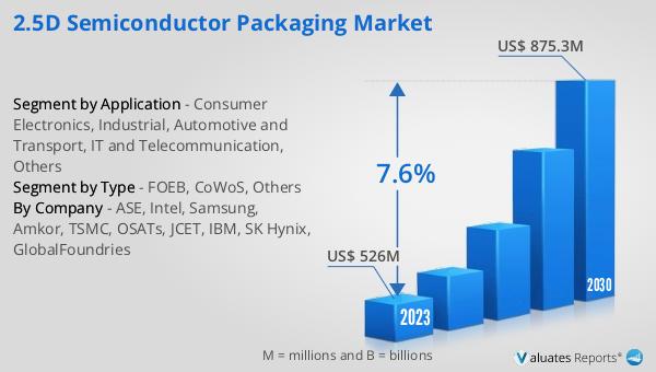
The global market for 2.5D semiconductor packaging was valued at $526 million in 2023 and is projected to reach $875.3 million by 2030, reflecting a compound annual growth rate (CAGR) of 7.6% during the forecast period from 2024 to 2030. This growth is driven by the increasing demand for high-performance and efficient semiconductor packaging solutions across various industries. The advancements in technology and the continuous development of new packaging methods are expected to contribute significantly to the market's expansion. The adoption of 2.5D semiconductor packaging is particularly strong in sectors such as consumer electronics, automotive, IT and telecommunications, and industrial applications. These industries require advanced packaging solutions to meet the growing demands for higher performance, reduced power consumption, and improved thermal management. The ability to integrate multiple chips on a single substrate allows for more functionality in a smaller footprint, making 2.5D packaging an attractive solution for a wide range of applications. As the demand for high-performance computing and advanced communication technologies continues to rise, the need for efficient and powerful semiconductor packaging solutions will become increasingly critical. The global market for 2.5D semiconductor packaging is expected to witness significant growth in the coming years, driven by the increasing adoption of advanced packaging technologies and the continuous improvement of existing ones. The future of the 2.5D semiconductor packaging market looks promising, with substantial growth anticipated during the forecast period.
| Report Metric | Details |
| Report Name | 2.5D Semiconductor Packaging Market |
| Accounted market size in 2023 | US$ 526 million |
| Forecasted market size in 2030 | US$ 875.3 million |
| CAGR | 7.6% |
| Base Year | 2023 |
| Forecasted years | 2024 - 2030 |
| Segment by Type |
|
| Segment by Application |
|
| By Region |
|
| By Company | ASE, Intel, Samsung, Amkor, TSMC, OSATs, JCET, IBM, SK Hynix, GlobalFoundries |
| Forecast units | USD million in value |
| Report coverage | Revenue and volume forecast, company share, competitive landscape, growth factors and trends |


