Thursday, January 30, 2025

Global Semiconductor Diffusion Furnace Market Research Report 2025

What is Global Semiconductor Diffusion Furnace Market?

The Global Semiconductor Diffusion Furnace Market is a crucial segment within the semiconductor manufacturing industry. This market focuses on the production and sale of diffusion furnaces, which are essential tools used in the fabrication of semiconductor devices. These furnaces are used to introduce impurities into semiconductor wafers, a process known as doping, which is vital for altering the electrical properties of the wafers to create integrated circuits and other semiconductor devices. The market is driven by the increasing demand for semiconductors across various industries, including consumer electronics, automotive, and telecommunications. As technology advances, the need for more efficient and precise diffusion processes grows, leading to innovations in furnace design and functionality. The market is characterized by a mix of established players and new entrants, all striving to offer advanced solutions that meet the evolving needs of semiconductor manufacturers. The growth of this market is closely linked to the overall expansion of the semiconductor industry, which continues to be fueled by the proliferation of smart devices, the Internet of Things (IoT), and the ongoing digital transformation across sectors.

Semiconductor Diffusion Furnace Market

Vertical Furnace, Horizontal Furnace in the Global Semiconductor Diffusion Furnace Market:

In the Global Semiconductor Diffusion Furnace Market, two primary types of furnaces are commonly used: vertical furnaces and horizontal furnaces. Vertical furnaces are designed with a vertical loading mechanism, where wafers are stacked vertically in a quartz tube. This design allows for better temperature uniformity and reduced contamination, making vertical furnaces ideal for processes that require high precision and cleanliness. They are often used in advanced semiconductor manufacturing processes, such as those involving smaller node technologies. Vertical furnaces are known for their efficiency in handling large wafer batches, which is crucial for high-volume production environments. On the other hand, horizontal furnaces feature a horizontal loading mechanism, where wafers are placed side by side in a horizontal tube. This design is typically more cost-effective and easier to maintain, making horizontal furnaces a popular choice for less complex processes or for manufacturers with budget constraints. Horizontal furnaces are often used in applications where the process requirements are less stringent, and they offer flexibility in handling different wafer sizes and types. Both vertical and horizontal furnaces play a significant role in the semiconductor diffusion process, each offering unique advantages that cater to specific manufacturing needs. The choice between vertical and horizontal furnaces depends on various factors, including the specific requirements of the semiconductor device being manufactured, the desired production volume, and the available budget. As the semiconductor industry continues to evolve, manufacturers are constantly seeking ways to optimize their diffusion processes, leading to ongoing innovations in furnace technology. These innovations aim to enhance process efficiency, improve wafer quality, and reduce operational costs. The competition between vertical and horizontal furnace manufacturers drives the development of new features and capabilities, such as improved temperature control, reduced energy consumption, and enhanced automation. As a result, the Global Semiconductor Diffusion Furnace Market is characterized by a dynamic landscape, where manufacturers must continuously adapt to meet the changing demands of the semiconductor industry.

Integrated Circuit, Optoelectronic Device, Others in the Global Semiconductor Diffusion Furnace Market:

The Global Semiconductor Diffusion Furnace Market finds its applications in various areas, including integrated circuits, optoelectronic devices, and other semiconductor components. In the realm of integrated circuits, diffusion furnaces are used to introduce dopants into silicon wafers, a critical step in the fabrication of transistors and other circuit elements. This process is essential for creating the electrical pathways that allow integrated circuits to function. The precision and uniformity offered by modern diffusion furnaces ensure that the dopants are evenly distributed, resulting in high-performance and reliable integrated circuits. In the field of optoelectronic devices, diffusion furnaces play a crucial role in the production of components such as LEDs, photodetectors, and laser diodes. These devices rely on precise doping to achieve the desired optical and electronic properties. The ability of diffusion furnaces to control the doping process with high accuracy is vital for producing optoelectronic devices that meet stringent performance standards. Additionally, diffusion furnaces are used in the manufacturing of other semiconductor components, such as power devices and sensors. These components often require specialized doping processes to achieve the necessary electrical characteristics. The versatility of diffusion furnaces allows manufacturers to tailor the doping process to meet the specific requirements of each component, ensuring optimal performance and reliability. As the demand for advanced semiconductor devices continues to grow, the Global Semiconductor Diffusion Furnace Market is poised to play an increasingly important role in enabling the production of cutting-edge technologies.

Global Semiconductor Diffusion Furnace Market Outlook:

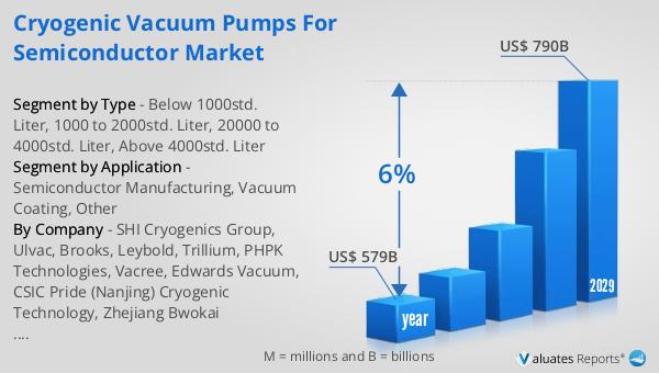
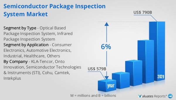
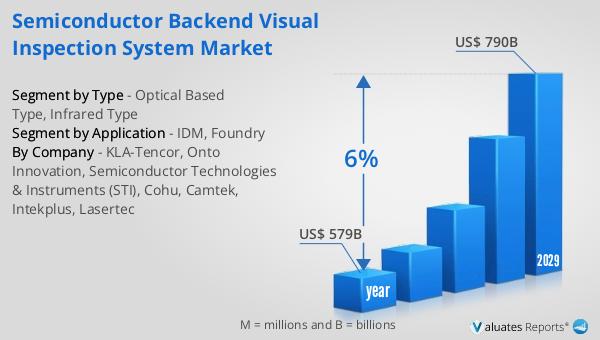
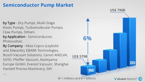
The global semiconductor market, valued at approximately $579 billion in 2022, is on a growth trajectory, with projections indicating it could reach around $790 billion by 2029. This anticipated growth represents a compound annual growth rate (CAGR) of 6% over the forecast period. This expansion is driven by the increasing demand for semiconductors across various industries, including consumer electronics, automotive, telecommunications, and more. The proliferation of smart devices, the Internet of Things (IoT), and the ongoing digital transformation across sectors are key factors fueling this demand. As technology continues to advance, the need for more efficient and precise semiconductor manufacturing processes becomes increasingly important. This, in turn, drives the demand for advanced diffusion furnaces, which are essential tools in the semiconductor fabrication process. The growth of the semiconductor market is closely linked to the innovations and advancements in diffusion furnace technology, as manufacturers strive to meet the evolving needs of the industry. As the market continues to expand, companies operating in the Global Semiconductor Diffusion Furnace Market are well-positioned to capitalize on the opportunities presented by this growth, offering advanced solutions that enhance the efficiency and precision of semiconductor manufacturing processes.


Report Metric Details
Report Name Semiconductor Diffusion Furnace Market
Accounted market size in year US$ 579 billion
Forecasted market size in 2029 US$ 790 billion
CAGR 6%
Base Year year
Forecasted years 2025 - 2029
by Type
  • Vertical Furnace
  • Horizontal Furnace
by Application
  • Integrated Circuit
  • Optoelectronic Device
  • Others
Production by Region
  • North America
  • Europe
  • China
  • Japan
Consumption by Region
  • North America (United States, Canada)
  • Europe (Germany, France, UK, Italy, Russia)
  • Asia-Pacific (China, Japan, South Korea, Taiwan)
  • Southeast Asia (India)
  • Latin America (Mexico, Brazil)
By Company BTU, Thermco Systems, Koyo Thermo Systems, JTEKT Thermo Systems, Ohkura, Beijing NAURA Microelectronics, Tokyo Electron, ASM International, CentrOthersm, SVCS Process Innovation, Tempress, SEMCO TECHNOLOGIES, Kokusai Electric Corporation
Forecast units USD million in value
Report coverage Revenue and volume forecast, company share, competitive landscape, growth factors and trends

Global Cryogenic Vacuum Pumps for Semiconductor Market Research Report 2025

What is Global Cryogenic Vacuum Pumps for Semiconductor Market?

The Global Cryogenic Vacuum Pumps for Semiconductor Market is a specialized segment within the broader semiconductor industry, focusing on the use of cryogenic vacuum pumps. These pumps are essential for creating and maintaining the ultra-low pressure environments required in semiconductor manufacturing processes. Cryogenic vacuum pumps operate at extremely low temperatures, often using liquid helium or nitrogen, to condense gases and remove them from the vacuum chamber. This technology is crucial for processes such as etching, deposition, and ion implantation, where even the slightest contamination can affect the quality and performance of semiconductor devices. The demand for cryogenic vacuum pumps is driven by the increasing complexity and miniaturization of semiconductor devices, which require more precise and controlled manufacturing environments. As the semiconductor industry continues to grow, fueled by advancements in technology and the proliferation of electronic devices, the market for cryogenic vacuum pumps is expected to expand, offering opportunities for innovation and development in this niche yet vital area of semiconductor manufacturing.

Cryogenic Vacuum Pumps for Semiconductor Market

Below 1000std. Liter, 1000 to 2000std. Liter, 20000 to 4000std. Liter, Above 4000std. Liter in the Global Cryogenic Vacuum Pumps for Semiconductor Market:

In the Global Cryogenic Vacuum Pumps for Semiconductor Market, the categorization based on pumping speed, measured in standard liters per second (std. L/s), is crucial for meeting the diverse needs of semiconductor manufacturing processes. Pumps with a capacity below 1000 std. L/s are typically used in applications requiring lower throughput and smaller vacuum chambers. These pumps are ideal for processes that do not demand high-speed evacuation but still require the precision and reliability of cryogenic technology. They are often employed in research and development settings or in the production of smaller semiconductor components where space and energy efficiency are paramount. Moving up the scale, pumps with a capacity between 1000 to 2000 std. L/s are more versatile and can handle a wider range of applications. These pumps are suitable for medium-sized vacuum chambers and are often used in batch processing environments where multiple wafers are processed simultaneously. They offer a balance between speed and efficiency, making them a popular choice for many semiconductor manufacturers. Pumps with a capacity between 2000 to 4000 std. L/s are designed for high-throughput applications where rapid evacuation of large volumes of gas is necessary. These pumps are typically used in large-scale manufacturing facilities where time is of the essence, and any delay can result in significant financial losses. They are essential for processes such as chemical vapor deposition and physical vapor deposition, where maintaining a stable and clean vacuum environment is critical. Finally, pumps with a capacity above 4000 std. L/s are the workhorses of the semiconductor industry, capable of handling the most demanding applications. These pumps are used in the largest vacuum chambers and are essential for processes that require the highest levels of precision and cleanliness. They are often employed in the production of advanced semiconductor devices, such as microprocessors and memory chips, where even the smallest impurity can lead to defects and reduced performance. The choice of pump capacity is determined by the specific requirements of the manufacturing process, including the size of the vacuum chamber, the type of gases being evacuated, and the desired level of vacuum. As the semiconductor industry continues to evolve, driven by the demand for smaller, faster, and more efficient devices, the need for advanced cryogenic vacuum pumps with higher capacities and improved performance will continue to grow.

Semiconductor Manufacturing, Vacuum Coating, Other in the Global Cryogenic Vacuum Pumps for Semiconductor Market:

The usage of Global Cryogenic Vacuum Pumps for Semiconductor Market spans several critical areas, including semiconductor manufacturing, vacuum coating, and other specialized applications. In semiconductor manufacturing, cryogenic vacuum pumps are indispensable for creating the ultra-clean environments necessary for producing high-quality semiconductor devices. These pumps are used in various stages of the manufacturing process, including etching, deposition, and ion implantation. During etching, for example, cryogenic vacuum pumps help maintain the low-pressure conditions required to precisely remove material from the wafer surface without introducing contaminants. Similarly, in deposition processes, these pumps ensure that the vacuum chamber remains free of impurities, allowing for the uniform application of thin films onto the wafer. The reliability and efficiency of cryogenic vacuum pumps are crucial for achieving the high yields and consistent quality demanded by the semiconductor industry. In vacuum coating applications, cryogenic vacuum pumps play a vital role in processes such as physical vapor deposition (PVD) and chemical vapor deposition (CVD). These processes are used to apply thin films of material onto various substrates, including semiconductor wafers, to enhance their properties or add functionality. Cryogenic vacuum pumps help maintain the low-pressure environments necessary for these coatings to adhere properly and achieve the desired thickness and uniformity. The ability to control the vacuum environment precisely is essential for producing coatings with the required optical, electrical, or mechanical properties. Beyond semiconductor manufacturing and vacuum coating, cryogenic vacuum pumps are used in other specialized applications where maintaining a clean and stable vacuum environment is critical. These applications can include research and development in fields such as materials science and nanotechnology, where precise control over the vacuum conditions is necessary for experimental accuracy. Additionally, cryogenic vacuum pumps are used in the production of advanced electronic devices, such as sensors and microelectromechanical systems (MEMS), where even minor contamination can affect performance and reliability. The versatility and effectiveness of cryogenic vacuum pumps make them an essential tool in a wide range of industries and applications, supporting the continued advancement of technology and innovation.

Global Cryogenic Vacuum Pumps for Semiconductor Market Outlook:

The global semiconductor market, valued at approximately US$ 579 billion in 2022, is on a growth trajectory, with projections indicating it could reach around US$ 790 billion by 2029. This growth represents a compound annual growth rate (CAGR) of 6% over the forecast period. The expansion of the semiconductor market is driven by several factors, including the increasing demand for electronic devices, advancements in technology, and the proliferation of applications requiring semiconductors, such as artificial intelligence, the Internet of Things (IoT), and 5G communications. As the demand for semiconductors continues to rise, the need for advanced manufacturing processes and equipment, including cryogenic vacuum pumps, becomes more critical. These pumps play a vital role in ensuring the quality and performance of semiconductor devices by maintaining the ultra-clean environments required during manufacturing. The growth of the semiconductor market presents significant opportunities for companies involved in the production and development of cryogenic vacuum pumps, as they are essential for meeting the stringent requirements of modern semiconductor manufacturing. As the industry evolves, driven by the demand for smaller, faster, and more efficient devices, the importance of cryogenic vacuum pumps in the semiconductor market is expected to increase, supporting the continued advancement of technology and innovation.


Report Metric Details
Report Name Cryogenic Vacuum Pumps for Semiconductor Market
Accounted market size in year US$ 579 billion
Forecasted market size in 2029 US$ 790 billion
CAGR 6%
Base Year year
Forecasted years 2025 - 2029
by Type
  • Below 1000std. Liter
  • 1000 to 2000std. Liter
  • 20000 to 4000std. Liter
  • Above 4000std. Liter
by Application
  • Semiconductor Manufacturing
  • Vacuum Coating
  • Other
Production by Region
  • North America
  • Europe
  • China
  • Japan
Consumption by Region
  • North America (United States, Canada)
  • Europe (Germany, France, UK, Italy, Russia)
  • Asia-Pacific (China, Japan, South Korea, Taiwan)
  • Southeast Asia (India)
  • Latin America (Mexico, Brazil)
By Company SHI Cryogenics Group, Ulvac, Brooks, Leybold, Trillium, PHPK Technologies, Vacree, Edwards Vacuum, CSIC Pride (Nanjing) Cryogenic Technology, Zhejiang Bwokai Electromechanical Technology, Suzhou Bama Superconductive Technology, Ultratorr Technology
Forecast units USD million in value
Report coverage Revenue and volume forecast, company share, competitive landscape, growth factors and trends

Global Semiconductor Package Inspection System Market Research Report 2025

What is Global Semiconductor Package Inspection System Market?

The Global Semiconductor Package Inspection System Market is a crucial segment within the semiconductor industry, focusing on the quality assurance of semiconductor packages. These systems are designed to inspect and ensure the integrity and functionality of semiconductor packages, which are essential components in electronic devices. The inspection systems utilize advanced technologies to detect defects, measure dimensions, and verify the quality of semiconductor packages. This market is driven by the increasing demand for high-performance and reliable electronic devices across various industries, including consumer electronics, automotive, industrial, and healthcare. As semiconductor technology advances, the complexity and miniaturization of semiconductor packages increase, necessitating more sophisticated inspection systems. The market is characterized by continuous innovation and development of new inspection technologies to meet the evolving needs of the semiconductor industry. Companies operating in this market are investing in research and development to enhance the accuracy, speed, and efficiency of their inspection systems. The Global Semiconductor Package Inspection System Market plays a vital role in ensuring the quality and reliability of semiconductor devices, which are integral to modern technology and everyday life.

Semiconductor Package Inspection System Market

Optical Based Package Inspection System, Infrared Package Inspection System in the Global Semiconductor Package Inspection System Market:

Optical-based package inspection systems are a significant component of the Global Semiconductor Package Inspection System Market. These systems use optical technologies, such as cameras and lasers, to inspect semiconductor packages for defects and ensure their quality. Optical inspection systems are known for their high precision and ability to detect even the smallest defects in semiconductor packages. They are widely used in the semiconductor industry due to their non-contact nature, which prevents damage to the delicate semiconductor packages during inspection. These systems can perform various inspections, including surface inspection, dimensional measurement, and alignment verification. The use of optical technologies allows for fast and accurate inspections, making them ideal for high-volume production environments. Infrared package inspection systems, on the other hand, utilize infrared technologies to inspect semiconductor packages. These systems are particularly useful for detecting defects that are not visible to the naked eye or through optical inspection. Infrared inspection systems can detect internal defects, such as voids or delaminations, within semiconductor packages. They work by analyzing the thermal properties of the packages, allowing for the detection of anomalies that may indicate defects. Infrared inspection systems are essential for ensuring the reliability and performance of semiconductor packages, especially in applications where high reliability is critical. Both optical and infrared package inspection systems are integral to the Global Semiconductor Package Inspection System Market, providing comprehensive inspection solutions to meet the diverse needs of the semiconductor industry. As the demand for more advanced and reliable semiconductor devices continues to grow, the importance of these inspection systems in ensuring the quality and performance of semiconductor packages becomes increasingly significant. Companies in this market are continuously innovating and developing new technologies to enhance the capabilities of their inspection systems, ensuring they can meet the evolving demands of the semiconductor industry.

Consumer Electronics, Automotive Electronics, Industrial, Healthcare, Others in the Global Semiconductor Package Inspection System Market:

The Global Semiconductor Package Inspection System Market finds extensive usage across various sectors, including consumer electronics, automotive electronics, industrial applications, healthcare, and others. In the consumer electronics sector, semiconductor package inspection systems are crucial for ensuring the quality and reliability of electronic devices such as smartphones, tablets, and laptops. These devices rely on high-performance semiconductor packages to function effectively, and any defects in these packages can lead to device failures. Inspection systems help manufacturers detect and rectify defects early in the production process, ensuring that only high-quality products reach the market. In the automotive electronics sector, semiconductor package inspection systems are used to ensure the reliability and safety of electronic components used in vehicles. Modern vehicles are equipped with numerous electronic systems, including infotainment systems, advanced driver-assistance systems (ADAS), and engine control units (ECUs), all of which rely on semiconductor packages. Inspection systems help ensure that these packages meet the stringent quality and safety standards required in the automotive industry. In industrial applications, semiconductor package inspection systems are used to ensure the quality of electronic components used in industrial machinery and equipment. These components are critical for the efficient and reliable operation of industrial systems, and any defects can lead to costly downtime and maintenance. Inspection systems help manufacturers maintain high-quality standards and reduce the risk of equipment failures. In the healthcare sector, semiconductor package inspection systems are used to ensure the reliability of electronic components used in medical devices. Medical devices, such as imaging systems, diagnostic equipment, and patient monitoring systems, rely on high-quality semiconductor packages to function accurately and reliably. Inspection systems help ensure that these packages meet the stringent quality standards required in the healthcare industry, ensuring patient safety and effective medical care. The Global Semiconductor Package Inspection System Market also finds applications in other sectors, such as telecommunications, aerospace, and defense, where the reliability and performance of semiconductor packages are critical. As technology continues to advance and the demand for high-performance electronic devices grows, the importance of semiconductor package inspection systems in ensuring the quality and reliability of semiconductor packages across various sectors becomes increasingly significant.

Global Semiconductor Package Inspection System Market Outlook:

The global semiconductor market was valued at approximately $579 billion in 2022 and is anticipated to reach around $790 billion by 2029, reflecting a compound annual growth rate (CAGR) of 6% over the forecast period. This growth is driven by the increasing demand for semiconductors across various industries, including consumer electronics, automotive, industrial, and healthcare. The rapid advancement of technology and the growing need for high-performance electronic devices are key factors contributing to the expansion of the semiconductor market. As the demand for more advanced and reliable semiconductor devices continues to rise, the importance of semiconductor package inspection systems in ensuring the quality and performance of these devices becomes increasingly significant. The Global Semiconductor Package Inspection System Market plays a vital role in supporting the growth of the semiconductor industry by providing advanced inspection solutions that help manufacturers maintain high-quality standards and meet the evolving demands of the market. Companies operating in this market are continuously innovating and developing new technologies to enhance the capabilities of their inspection systems, ensuring they can meet the growing needs of the semiconductor industry. As the semiconductor market continues to expand, the demand for advanced inspection systems is expected to increase, further driving the growth of the Global Semiconductor Package Inspection System Market.


Report Metric Details
Report Name Semiconductor Package Inspection System Market
Accounted market size in year US$ 579 billion
Forecasted market size in 2029 US$ 790 billion
CAGR 6%
Base Year year
Forecasted years 2025 - 2029
by Type
  • Optical Based Package Inspection System
  • Infrared Package Inspection System
by Application
  • Consumer Electronics
  • Automotive Electronics
  • Industrial
  • Healthcare
  • Others
Production by Region
  • North America
  • Europe
  • China
  • Japan
Consumption by Region
  • North America (United States, Canada)
  • Europe (Germany, France, UK, Italy, Russia)
  • Asia-Pacific (China, Japan, South Korea, Taiwan)
  • Southeast Asia (India)
  • Latin America (Mexico, Brazil)
By Company KLA-Tencor, Onto Innovation, Semiconductor Technologies & Instruments (STI), Cohu, Camtek, Intekplus
Forecast units USD million in value
Report coverage Revenue and volume forecast, company share, competitive landscape, growth factors and trends

Global Semiconductor Backend Visual Inspection System Market Research Report 2025

What is Global Semiconductor Backend Visual Inspection System Market?

The Global Semiconductor Backend Visual Inspection System Market is a crucial segment within the semiconductor industry, focusing on the inspection of semiconductor devices after the manufacturing process. This market involves systems that are designed to detect defects and ensure the quality of semiconductor products before they are shipped to customers. These systems are essential for maintaining high standards of quality and reliability in semiconductor devices, which are used in a wide range of applications, from consumer electronics to automotive and industrial equipment. The market is driven by the increasing demand for semiconductors, the complexity of semiconductor devices, and the need for high precision and accuracy in inspection processes. As semiconductor technology continues to advance, the demand for more sophisticated and efficient inspection systems is expected to grow, making this market a vital component of the semiconductor supply chain. The systems used in this market employ various technologies, including optical and infrared inspection, to identify defects that could affect the performance and reliability of semiconductor devices. By ensuring that only high-quality products reach the market, these systems help manufacturers maintain their reputation and meet the stringent requirements of their customers.

Semiconductor Backend Visual Inspection System Market

Optical Based Type, Infrared Type in the Global Semiconductor Backend Visual Inspection System Market:

In the Global Semiconductor Backend Visual Inspection System Market, two prominent types of inspection technologies are Optical-Based and Infrared-Based systems. Optical-Based inspection systems utilize visible light to examine semiconductor devices for defects. These systems are equipped with high-resolution cameras and advanced image processing software to detect surface defects, such as scratches, cracks, and contamination, that could compromise the performance of the semiconductor device. The advantage of optical inspection is its ability to provide detailed images of the device surface, allowing for precise identification and classification of defects. This type of inspection is particularly useful for detecting defects that are visible to the naked eye and for ensuring the overall quality of the semiconductor device. On the other hand, Infrared-Based inspection systems use infrared light to penetrate the semiconductor material and detect internal defects that are not visible on the surface. This technology is essential for identifying issues such as voids, delamination, and other internal anomalies that could affect the structural integrity and functionality of the semiconductor device. Infrared inspection is particularly valuable for inspecting complex semiconductor devices with multiple layers, as it can provide a comprehensive view of the internal structure without damaging the device. Both Optical-Based and Infrared-Based inspection systems play a critical role in the semiconductor manufacturing process, ensuring that devices meet the required quality standards and perform reliably in their intended applications. As the demand for more advanced and miniaturized semiconductor devices continues to grow, the need for sophisticated inspection systems that can accurately detect and classify defects is becoming increasingly important. Manufacturers are investing in the development of new inspection technologies and improving existing systems to enhance their capabilities and meet the evolving needs of the semiconductor industry. By leveraging these advanced inspection systems, manufacturers can improve their production yields, reduce costs, and deliver high-quality products to their customers. The integration of artificial intelligence and machine learning technologies into inspection systems is also gaining traction, enabling more efficient and accurate defect detection and classification. These advancements are expected to drive the growth of the Global Semiconductor Backend Visual Inspection System Market, as manufacturers seek to enhance their inspection capabilities and maintain their competitive edge in the rapidly evolving semiconductor industry.

IDM, Foundry in the Global Semiconductor Backend Visual Inspection System Market:

The Global Semiconductor Backend Visual Inspection System Market finds significant usage in Integrated Device Manufacturers (IDMs) and Foundries, two key players in the semiconductor industry. IDMs are companies that design, manufacture, and sell semiconductor devices, handling the entire production process from start to finish. For IDMs, visual inspection systems are crucial for ensuring the quality and reliability of their products. These systems help IDMs identify defects early in the production process, allowing them to address issues before they affect the final product. By maintaining high-quality standards, IDMs can enhance their reputation and meet the stringent requirements of their customers. Visual inspection systems also enable IDMs to optimize their production processes, reduce waste, and improve yields, ultimately leading to cost savings and increased profitability. Foundries, on the other hand, are companies that specialize in manufacturing semiconductor devices for other companies, known as fabless companies, which design but do not manufacture their own chips. For foundries, visual inspection systems are essential for meeting the quality standards set by their clients and ensuring the reliability of the semiconductor devices they produce. These systems help foundries detect defects and anomalies in the manufacturing process, allowing them to make necessary adjustments and maintain high production yields. By delivering high-quality products, foundries can strengthen their relationships with clients and secure long-term contracts. Visual inspection systems also enable foundries to stay competitive in the market by adopting the latest technologies and improving their manufacturing capabilities. As the semiconductor industry continues to evolve, both IDMs and foundries are investing in advanced visual inspection systems to enhance their inspection capabilities and meet the growing demand for high-quality semiconductor devices. The integration of new technologies, such as artificial intelligence and machine learning, into visual inspection systems is helping IDMs and foundries improve their defect detection and classification processes, leading to more efficient and accurate inspections. By leveraging these advanced systems, IDMs and foundries can maintain their competitive edge in the rapidly changing semiconductor industry and continue to deliver high-quality products to their customers.

Global Semiconductor Backend Visual Inspection System Market Outlook:

The global semiconductor market, valued at approximately $579 billion in 2022, is anticipated to reach around $790 billion by 2029, reflecting a compound annual growth rate (CAGR) of 6% over the forecast period. This growth is indicative of the increasing demand for semiconductors across various industries, driven by advancements in technology and the proliferation of electronic devices. Semiconductors are integral components in a wide range of applications, from consumer electronics and telecommunications to automotive and industrial equipment. The rising adoption of technologies such as artificial intelligence, the Internet of Things (IoT), and 5G is further fueling the demand for semiconductors, as these technologies require advanced and efficient semiconductor devices to function effectively. As the market continues to expand, manufacturers are investing in research and development to innovate and produce more sophisticated semiconductor devices that meet the evolving needs of their customers. The growth of the semiconductor market also highlights the importance of maintaining high-quality standards and ensuring the reliability of semiconductor devices. This is where the Global Semiconductor Backend Visual Inspection System Market plays a crucial role, as it provides the necessary tools and technologies to inspect and verify the quality of semiconductor devices before they reach the market. By leveraging advanced inspection systems, manufacturers can improve their production yields, reduce costs, and deliver high-quality products to their customers, ultimately contributing to the overall growth and success of the semiconductor industry.


Report Metric Details
Report Name Semiconductor Backend Visual Inspection System Market
Accounted market size in year US$ 579 billion
Forecasted market size in 2029 US$ 790 billion
CAGR 6%
Base Year year
Forecasted years 2025 - 2029
by Type
  • Optical Based Type
  • Infrared Type
by Application
  • IDM
  • Foundry
Production by Region
  • North America
  • Europe
  • China
  • Japan
Consumption by Region
  • North America (United States, Canada)
  • Europe (Germany, France, UK, Italy, Russia)
  • Asia-Pacific (China, Japan, South Korea, Taiwan)
  • Southeast Asia (India)
  • Latin America (Mexico, Brazil)
By Company KLA-Tencor, Onto Innovation, Semiconductor Technologies & Instruments (STI), Cohu, Camtek, Intekplus, Lasertec
Forecast units USD million in value
Report coverage Revenue and volume forecast, company share, competitive landscape, growth factors and trends

Global Vaccine Monitoring Data Logger Market Research Report 2025

What is Global Vaccine Monitoring Data Logger Market?

The Global Vaccine Monitoring Data Logger Market is a specialized segment within the broader data logger industry, focusing on the precise monitoring of vaccine storage conditions. These data loggers are essential tools used to ensure that vaccines are stored and transported under optimal conditions, maintaining their efficacy and safety. They record and track temperature, humidity, and other environmental parameters, providing real-time data and alerts if conditions deviate from the required standards. This market has gained significant importance due to the increasing demand for vaccines worldwide, driven by public health initiatives and the need to combat infectious diseases. The data loggers help in maintaining the cold chain, a critical component in vaccine distribution, ensuring that vaccines remain effective from the point of manufacture to administration. With advancements in technology, these devices have become more sophisticated, offering wireless connectivity, cloud storage, and enhanced data analytics capabilities. The market is characterized by a range of products, from simple USB data loggers to advanced wireless systems, catering to various needs and budgets. As global vaccination efforts continue to expand, the demand for reliable and efficient vaccine monitoring data loggers is expected to grow, highlighting their crucial role in public health.

Vaccine Monitoring Data Logger Market

Wireless Data Logger, Wired Data Logger in the Global Vaccine Monitoring Data Logger Market:

In the Global Vaccine Monitoring Data Logger Market, data loggers are categorized into two main types: wireless and wired. Wireless data loggers are increasingly popular due to their convenience and advanced features. These devices use wireless technology, such as Wi-Fi, Bluetooth, or cellular networks, to transmit data to a central system or cloud-based platform. This allows for real-time monitoring and alerts, enabling quick responses to any deviations in storage conditions. Wireless data loggers are particularly useful in large-scale operations where multiple storage units need to be monitored simultaneously. They offer the flexibility of remote access, allowing users to check data and receive alerts from anywhere, which is crucial for maintaining the integrity of vaccines during transportation and storage. Additionally, wireless data loggers often come with advanced features like GPS tracking, which is beneficial for monitoring the location and condition of vaccines in transit. On the other hand, wired data loggers are traditional devices that require a physical connection to download data. They are typically connected to a computer or a central monitoring system via USB or Ethernet cables. While they may lack the convenience of wireless data transmission, wired data loggers are known for their reliability and accuracy. They are often used in fixed locations where constant monitoring is required, such as in hospitals, laboratories, and storage facilities. Wired data loggers are generally more cost-effective than their wireless counterparts, making them a viable option for smaller operations or facilities with budget constraints. Despite their limitations in terms of mobility and remote access, wired data loggers provide a stable and secure means of data collection, ensuring that critical information is accurately recorded and stored. Both wireless and wired data loggers play a vital role in the Global Vaccine Monitoring Data Logger Market, each offering unique advantages depending on the specific needs of the user. Wireless data loggers are ideal for dynamic environments where flexibility and real-time data access are paramount. They are particularly beneficial in scenarios where vaccines are frequently moved or where multiple locations need to be monitored simultaneously. The ability to receive instant alerts and access data remotely can significantly enhance the efficiency of vaccine management, reducing the risk of spoilage and ensuring that vaccines remain effective. Conversely, wired data loggers are best suited for static environments where the focus is on long-term monitoring and data accuracy. They provide a dependable solution for facilities that require continuous monitoring without the need for frequent data retrieval or remote access. The simplicity and cost-effectiveness of wired data loggers make them an attractive option for smaller healthcare providers or organizations with limited resources. Despite the growing popularity of wireless technology, wired data loggers continue to hold a significant share of the market due to their proven reliability and ease of use. In conclusion, the choice between wireless and wired data loggers in the Global Vaccine Monitoring Data Logger Market depends largely on the specific requirements of the user. Both types of data loggers offer valuable solutions for ensuring the safe storage and transportation of vaccines, contributing to the overall success of vaccination programs worldwide. As technology continues to evolve, it is likely that both wireless and wired data loggers will continue to play a crucial role in the effective management of vaccine storage conditions, supporting global efforts to improve public health and combat infectious diseases.

Hospital, Epidemic Prevention Station, Others in the Global Vaccine Monitoring Data Logger Market:

The Global Vaccine Monitoring Data Logger Market finds extensive usage in various sectors, including hospitals, epidemic prevention stations, and other healthcare facilities. In hospitals, these data loggers are crucial for maintaining the integrity of vaccines stored in refrigerators and freezers. Hospitals often have large inventories of vaccines that need to be stored at specific temperatures to remain effective. Data loggers provide continuous monitoring of these storage conditions, ensuring that any deviations are quickly identified and addressed. This is particularly important in hospital settings where vaccines are administered to vulnerable populations, such as infants, the elderly, and immunocompromised patients. By ensuring that vaccines are stored correctly, hospitals can provide safe and effective immunizations, reducing the risk of vaccine-preventable diseases. Epidemic prevention stations also rely heavily on vaccine monitoring data loggers to manage their vaccine supplies. These stations are often at the forefront of public health efforts, working to prevent the spread of infectious diseases through vaccination campaigns. Data loggers help ensure that vaccines are stored and transported under optimal conditions, maintaining their potency and effectiveness. This is especially important during outbreaks when large quantities of vaccines need to be distributed quickly and efficiently. By using data loggers, epidemic prevention stations can monitor the temperature and humidity levels of their storage facilities, ensuring that vaccines remain viable throughout the distribution process. This not only helps prevent vaccine spoilage but also ensures that vaccination efforts are successful in controlling the spread of diseases. In addition to hospitals and epidemic prevention stations, other healthcare facilities also benefit from the use of vaccine monitoring data loggers. These facilities may include clinics, pharmacies, and research laboratories, all of which require precise temperature control for their vaccine supplies. Data loggers provide a reliable means of monitoring storage conditions, helping to prevent vaccine wastage and ensuring that patients receive effective immunizations. In research laboratories, data loggers are used to monitor the storage conditions of experimental vaccines, ensuring that they remain stable and effective throughout the research process. This is crucial for the development of new vaccines and the advancement of public health initiatives. Overall, the Global Vaccine Monitoring Data Logger Market plays a vital role in ensuring the safe storage and transportation of vaccines across various healthcare settings. By providing accurate and reliable data on storage conditions, these devices help maintain the efficacy of vaccines, supporting global efforts to improve public health and prevent the spread of infectious diseases. As vaccination programs continue to expand worldwide, the demand for effective vaccine monitoring solutions is expected to grow, highlighting the importance of data loggers in the healthcare industry.

Global Vaccine Monitoring Data Logger Market Outlook:

The outlook for the Global Vaccine Monitoring Data Logger Market can be contextualized by examining the broader pharmaceutical and chemical drug markets. In 2022, the global pharmaceutical market was valued at approximately 1,475 billion USD, with an anticipated compound annual growth rate (CAGR) of 5% over the next six years. This growth is indicative of the increasing demand for pharmaceutical products, including vaccines, which in turn drives the need for effective monitoring solutions to ensure their safety and efficacy. In comparison, the chemical drug market has shown a steady increase, growing from 1,005 billion USD in 2018 to an estimated 1,094 billion USD in 2022. This growth reflects the ongoing demand for chemical-based medications, which, like vaccines, require precise storage conditions to maintain their effectiveness. The expansion of these markets underscores the critical role of data loggers in maintaining the integrity of pharmaceutical products. As the demand for vaccines and other medications continues to rise, the need for reliable monitoring solutions becomes increasingly important. Data loggers provide a means of ensuring that these products are stored and transported under optimal conditions, preventing spoilage and ensuring that patients receive safe and effective treatments. The growth of the pharmaceutical and chemical drug markets highlights the importance of investing in advanced monitoring technologies, such as wireless and wired data loggers, to support the safe distribution of these products. In conclusion, the Global Vaccine Monitoring Data Logger Market is poised to benefit from the ongoing growth of the pharmaceutical and chemical drug markets. As these industries continue to expand, the demand for effective monitoring solutions will likely increase, driving innovation and development in the data logger market. By providing accurate and reliable data on storage conditions, data loggers play a crucial role in ensuring the safety and efficacy of vaccines and other pharmaceutical products, supporting global efforts to improve public health and combat infectious diseases.


Report Metric Details
Report Name Vaccine Monitoring Data Logger Market
CAGR 5%
by Type
  • Wireless Data Logger
  • Wired Data Logger
by Application
  • Hospital
  • Epidemic Prevention Station
  • Others
Production by Region
  • North America
  • Europe
  • China
  • Japan
Consumption by Region
  • North America (United States, Canada)
  • Europe (Germany, France, UK, Italy, Russia)
  • Asia-Pacific (China, Japan, South Korea, Taiwan)
  • Southeast Asia (India)
  • Latin America (Mexico, Brazil)
By Company Elitech, Lascar Electronics, Control Solutions, T&D Corporation, SpotSee, PCE Instruments, MadgeTech, B Medical, Testo, Traceable, Elpro, Electronic Temperature Instruments, AccuVax, FilesThruTheAir
Forecast units USD million in value
Report coverage Revenue and volume forecast, company share, competitive landscape, growth factors and trends

Global X-ray Food & Pharmaceutical Inspection System Market Research Report 2025

What is Global X-ray Food & Pharmaceutical Inspection System Market?

The Global X-ray Food & Pharmaceutical Inspection System Market is a specialized segment within the broader inspection systems industry, focusing on the use of X-ray technology to ensure the safety and quality of food and pharmaceutical products. These systems are designed to detect contaminants, such as metal, glass, stone, and other foreign materials, that may be present in packaged or bulk products. The technology is highly valued for its ability to provide non-destructive testing, meaning it can inspect products without damaging them, which is crucial for maintaining product integrity. In the food industry, X-ray inspection systems help in identifying physical contaminants and ensuring compliance with safety standards, thereby protecting consumers and brands alike. In the pharmaceutical sector, these systems are used to verify the integrity of tablets, capsules, and other products, ensuring they are free from contaminants and defects. The market for these systems is driven by increasing regulatory requirements, consumer demand for safe products, and the need for manufacturers to maintain high-quality standards. As industries continue to prioritize safety and quality, the demand for advanced inspection technologies like X-ray systems is expected to grow, making this market an essential component of the global food and pharmaceutical supply chains.

X-ray Food & Pharmaceutical Inspection System Market

Packaged Product Inspection Equipment, Bulk Product Inspection Equipment in the Global X-ray Food & Pharmaceutical Inspection System Market:

Packaged Product Inspection Equipment and Bulk Product Inspection Equipment are two critical components of the Global X-ray Food & Pharmaceutical Inspection System Market. Packaged Product Inspection Equipment is specifically designed to inspect products that are already packaged, such as boxed, bagged, or bottled goods. These systems are crucial in ensuring that the final product reaching the consumer is free from any physical contaminants. They work by scanning the packaged goods and using advanced algorithms to detect any anomalies that might indicate the presence of foreign materials. This type of equipment is widely used in both the food and pharmaceutical industries, where the integrity of the packaging and the safety of the contents are paramount. For instance, in the food industry, packaged product inspection equipment can detect contaminants like metal shards or glass pieces that might have accidentally entered during the packaging process. In the pharmaceutical industry, these systems ensure that tablets or capsules are correctly filled and free from defects or contaminants before they are sealed and shipped. On the other hand, Bulk Product Inspection Equipment is used to inspect products in bulk form before they are packaged. This type of equipment is essential for industries that deal with raw materials or products that are processed in large quantities. In the food industry, bulk product inspection equipment is used to scan items like grains, nuts, or meat products to detect any foreign objects before they are processed further or packaged. This ensures that any contaminants are removed early in the production process, reducing the risk of them ending up in the final product. In the pharmaceutical industry, bulk inspection equipment is used to inspect raw materials like powders or granules to ensure they meet the required safety and quality standards before they are used in the production of medicines. Both types of inspection equipment play a vital role in maintaining the safety and quality of products in the food and pharmaceutical industries. They help manufacturers comply with stringent regulatory requirements and meet consumer expectations for safe and high-quality products. The choice between packaged and bulk inspection equipment depends on the specific needs of the manufacturer and the stage of the production process where inspection is most critical. As technology advances, these systems are becoming more sophisticated, with features like real-time data analysis, automated reporting, and integration with other quality control systems. This not only enhances their efficiency but also provides manufacturers with valuable insights into their production processes, helping them to identify and address potential issues before they become major problems. Overall, the Global X-ray Food & Pharmaceutical Inspection System Market is a dynamic and evolving sector that plays a crucial role in ensuring the safety and quality of products that consumers rely on every day.

Food, Pharmaceutical in the Global X-ray Food & Pharmaceutical Inspection System Market:

The usage of Global X-ray Food & Pharmaceutical Inspection System Market in the food and pharmaceutical sectors is extensive and multifaceted. In the food industry, X-ray inspection systems are employed at various stages of the production process to ensure that the final product is safe for consumption. These systems are capable of detecting a wide range of contaminants, including metal, glass, stone, and even some types of plastic, which might be present in food products due to accidental contamination during processing or packaging. By identifying and removing these contaminants, X-ray inspection systems help manufacturers comply with food safety regulations and protect consumers from potential health hazards. Additionally, these systems can also be used to check the integrity of packaging, ensuring that products are sealed correctly and free from defects that could compromise their quality or safety. In the pharmaceutical industry, X-ray inspection systems are used to ensure the safety and quality of medicines and other healthcare products. These systems are capable of inspecting tablets, capsules, and other pharmaceutical products to detect any foreign materials or defects that might affect their efficacy or safety. For example, X-ray inspection systems can identify broken tablets, missing components, or incorrect fill levels in blister packs, ensuring that only products that meet the required quality standards are released to the market. This is particularly important in the pharmaceutical industry, where even minor defects can have serious implications for patient safety and product efficacy. Moreover, X-ray inspection systems can also be used to verify the integrity of packaging, ensuring that products are protected from contamination and tampering. The use of X-ray inspection systems in both the food and pharmaceutical industries is driven by the need to comply with stringent regulatory requirements and meet consumer expectations for safe and high-quality products. These systems provide manufacturers with a reliable and efficient way to detect and remove contaminants, ensuring that their products meet the highest safety and quality standards. Furthermore, the data collected by these systems can be used to improve production processes, identify potential issues, and implement corrective actions, helping manufacturers to maintain their competitive edge in the market. As technology continues to advance, X-ray inspection systems are becoming more sophisticated, with features like real-time data analysis, automated reporting, and integration with other quality control systems. This not only enhances their efficiency but also provides manufacturers with valuable insights into their production processes, helping them to identify and address potential issues before they become major problems. Overall, the Global X-ray Food & Pharmaceutical Inspection System Market plays a crucial role in ensuring the safety and quality of products that consumers rely on every day.

Global X-ray Food & Pharmaceutical Inspection System Market Outlook:

In 2022, the global pharmaceutical market reached a valuation of 1,475 billion USD, demonstrating a steady growth trajectory with a compound annual growth rate (CAGR) of 5% projected over the next six years. This growth reflects the increasing demand for pharmaceutical products worldwide, driven by factors such as an aging population, rising prevalence of chronic diseases, and advancements in medical technology. In comparison, the chemical drug market has also shown significant growth, expanding from 1,005 billion USD in 2018 to 1,094 billion USD in 2022. This increase highlights the ongoing importance of chemical drugs in the global healthcare landscape, despite the growing interest in biologics and other innovative therapies. The expansion of both the pharmaceutical and chemical drug markets underscores the critical role of inspection systems in ensuring the safety and quality of these products. As the demand for pharmaceutical products continues to rise, manufacturers are under increasing pressure to comply with stringent regulatory requirements and meet consumer expectations for safe and effective medicines. This has led to a growing reliance on advanced inspection technologies, such as X-ray systems, to detect and remove contaminants, verify product integrity, and ensure compliance with industry standards. As a result, the Global X-ray Food & Pharmaceutical Inspection System Market is poised to play an increasingly important role in supporting the growth and development of the pharmaceutical industry.


Report Metric Details
Report Name X-ray Food & Pharmaceutical Inspection System Market
CAGR 5%
by Type
  • Packaged Product Inspection Equipment
  • Bulk Product Inspection Equipment
by Application
  • Food
  • Pharmaceutical
Production by Region
  • North America
  • Europe
  • China
  • Japan
Consumption by Region
  • North America (United States, Canada)
  • Europe (Germany, France, UK, Italy, Russia)
  • Asia-Pacific (China, Japan, South Korea, Taiwan)
  • Southeast Asia (India)
  • Latin America (Mexico, Brazil)
By Company Anritsu Infivis, Mettler-Toledo, Minebea Intec, Thermo-fisher, Ishida, Loma Systems, Sesotec GmbH, Multivac Group, Dylog Hi-Tech, Bizerba, Techik, WIPOTEC-OCS, Mekitec, NongShim Engineering, Meyer, COSO, SHANAN, Gaojing, JUZHENG Electronic and Technology, Easyweigh
Forecast units USD million in value
Report coverage Revenue and volume forecast, company share, competitive landscape, growth factors and trends

Global Semiconductor Pump Market Research Report 2025

What is Global Semiconductor Pump Market?

The Global Semiconductor Pump Market is a crucial segment within the broader semiconductor industry, focusing on the production and distribution of pumps specifically designed for semiconductor manufacturing processes. These pumps are essential for maintaining the vacuum and controlled environments required in semiconductor fabrication, which involves intricate processes like etching, deposition, and cleaning. The market encompasses a variety of pump types, each tailored to specific applications within the semiconductor manufacturing process. As the demand for semiconductors continues to rise, driven by advancements in technology and increasing applications in various sectors such as consumer electronics, automotive, and telecommunications, the semiconductor pump market is experiencing significant growth. This growth is further fueled by the ongoing miniaturization of semiconductor devices, which necessitates more precise and efficient manufacturing processes. Consequently, manufacturers in this market are continually innovating to develop pumps that offer higher efficiency, reliability, and performance to meet the evolving needs of the semiconductor industry. The global semiconductor pump market is thus a dynamic and rapidly evolving sector, playing a pivotal role in supporting the technological advancements and production capabilities of the semiconductor industry worldwide.

Semiconductor Pump Market

Dry Pumps, Multi-Stage Roots Pumps, Turbomolecular Pumps, Claw Pumps, Others in the Global Semiconductor Pump Market:

In the Global Semiconductor Pump Market, various types of pumps are utilized, each serving a unique purpose in the semiconductor manufacturing process. Dry pumps, for instance, are widely used due to their ability to operate without any lubricating fluids, which minimizes the risk of contamination in sensitive semiconductor processes. These pumps are particularly valued for their low maintenance requirements and high reliability, making them ideal for continuous operation in demanding environments. Multi-stage roots pumps, on the other hand, are known for their ability to handle large volumes of gas at low pressures, making them suitable for applications that require rapid evacuation of chambers. Their design allows for efficient operation with minimal energy consumption, which is a critical consideration in the energy-intensive semiconductor manufacturing process. Turbomolecular pumps are another essential component in the semiconductor pump market, renowned for their ability to achieve extremely high vacuum levels. These pumps are crucial in processes that require ultra-clean environments, such as the deposition of thin films and the etching of intricate patterns on semiconductor wafers. Their precision and efficiency make them indispensable in the production of high-performance semiconductor devices. Claw pumps, meanwhile, are appreciated for their robustness and ability to handle corrosive gases, which are often encountered in semiconductor manufacturing. Their design ensures minimal wear and tear, contributing to their longevity and reliability in harsh operating conditions. Lastly, the category of 'Others' in the semiconductor pump market includes a variety of specialized pumps that cater to niche applications within the industry. These may include diaphragm pumps, scroll pumps, and other custom-designed solutions that address specific challenges in semiconductor manufacturing. Each type of pump plays a vital role in ensuring the efficiency, precision, and reliability of semiconductor production processes, highlighting the diverse and specialized nature of the global semiconductor pump market.

Semiconductor, Photovoltaic in the Global Semiconductor Pump Market:

The Global Semiconductor Pump Market finds extensive usage in the semiconductor and photovoltaic industries, each with its unique requirements and challenges. In the semiconductor industry, pumps are integral to maintaining the vacuum and controlled environments necessary for various fabrication processes. These processes include chemical vapor deposition, physical vapor deposition, and etching, all of which require precise control over pressure and gas flow to ensure the quality and performance of the final semiconductor products. Pumps such as turbomolecular and dry pumps are particularly critical in these applications, as they provide the high vacuum levels and contamination-free environments needed for the production of advanced semiconductor devices. The reliability and efficiency of these pumps directly impact the yield and quality of semiconductor wafers, making them indispensable in the industry. In the photovoltaic industry, semiconductor pumps are used in the production of solar cells, where they play a crucial role in processes such as thin-film deposition and plasma-enhanced chemical vapor deposition. These processes require precise control over the deposition environment to ensure the uniformity and efficiency of the photovoltaic cells. Pumps like multi-stage roots and claw pumps are often employed in these applications due to their ability to handle large volumes of gas and corrosive materials, which are common in photovoltaic manufacturing. The efficiency and performance of these pumps are vital in optimizing the production process and reducing the overall cost of photovoltaic cells, thereby contributing to the competitiveness of solar energy as a renewable energy source. Overall, the global semiconductor pump market is essential in supporting the technological advancements and production capabilities of both the semiconductor and photovoltaic industries, enabling the development of high-performance electronic and renewable energy solutions.

Global Semiconductor Pump Market Outlook:

The global semiconductor market, valued at approximately $579 billion in 2022, is on a trajectory to reach around $790 billion by 2029, reflecting a compound annual growth rate (CAGR) of 6% over the forecast period. This growth is indicative of the increasing demand for semiconductors across various sectors, driven by technological advancements and the proliferation of electronic devices. The semiconductor industry is a cornerstone of modern technology, underpinning innovations in areas such as artificial intelligence, the Internet of Things (IoT), and 5G communications. As these technologies continue to evolve and integrate into everyday life, the demand for semiconductors is expected to rise correspondingly. The projected growth of the semiconductor market underscores the critical role that semiconductors play in enabling technological progress and economic development. This expansion is also likely to drive further advancements in semiconductor manufacturing processes, including the development of more efficient and reliable semiconductor pumps, which are essential for maintaining the precision and quality of semiconductor products. As the market continues to grow, companies within the semiconductor pump market will need to innovate and adapt to meet the evolving needs of the semiconductor industry, ensuring that they can support the increasing demand for high-performance semiconductor devices.


Report Metric Details
Report Name Semiconductor Pump Market
Accounted market size in year US$ 579 billion
Forecasted market size in 2029 US$ 790 billion
CAGR 6%
Base Year year
Forecasted years 2025 - 2029
by Type
  • Dry Pumps
  • Multi-Stage Roots Pumps
  • Turbomolecular Pumps
  • Claw Pumps
  • Others
by Application
  • Semiconductor
  • Photovoltaic
Production by Region
  • North America
  • Europe
  • China
  • Japan
Consumption by Region
  • North America (United States, Canada)
  • Europe (Germany, France, UK, Italy, Russia)
  • Asia-Pacific (China, Japan, South Korea, Taiwan)
  • Southeast Asia (India)
  • Latin America (Mexico, Brazil)
By Company Atlas Copco (Leybold and Edwards), EBARA Technologies, Busch Vacuum Solutions, Canon ANELVA, SATO, Pfeiffer Vacuum, Kashiyama Europe GmbH, Everest Vacuum, Shanghai Hanbell Precise Machinery, SKY Technology Development, Edwards Vacuum, Levitronix, IWAKI, Dellmeco GmbH, DL Thurrott, Pneumofore
Forecast units USD million in value
Report coverage Revenue and volume forecast, company share, competitive landscape, growth factors and trends

Global Berberine Chloride API Market Research Report 2025

What is Global Berberine Chloride API Market? The Global Berberine Chloride API Market is a specialized segment within the pharmaceutical a...