What is Global Semiconductor Lens Market?
The Global Semiconductor Lens Market is a crucial component of the semiconductor industry, which plays a vital role in the production of electronic devices. Semiconductor lenses are specialized optical components used in the manufacturing process of semiconductors, particularly in photolithography, where they help in projecting circuit patterns onto silicon wafers. These lenses are essential for achieving the high precision and accuracy required in the production of microchips. The market for semiconductor lenses is driven by the increasing demand for advanced electronic devices, such as smartphones, tablets, and computers, which require sophisticated and miniaturized semiconductor components. Additionally, the rise of technologies like artificial intelligence, the Internet of Things (IoT), and 5G connectivity further fuels the demand for high-performance semiconductors, thereby boosting the need for advanced semiconductor lenses. As the semiconductor industry continues to evolve, the demand for more efficient and precise lenses is expected to grow, making the Global Semiconductor Lens Market a dynamic and rapidly developing sector. The market is characterized by continuous innovation and technological advancements, as manufacturers strive to meet the ever-increasing demands of the electronics industry.
DUV Lithography Lens, EUV Lithography Lens in the Global Semiconductor Lens Market:
In the realm of semiconductor manufacturing, DUV (Deep Ultraviolet) and EUV (Extreme Ultraviolet) lithography lenses are pivotal technologies that have revolutionized the production of microchips. DUV lithography lenses operate at wavelengths of 193 nanometers and are widely used in the semiconductor industry for producing chips with smaller and more complex features. These lenses are integral to the photolithography process, where they focus light onto a photoresist-coated silicon wafer to create intricate circuit patterns. The precision and accuracy of DUV lenses are crucial for achieving the high-resolution patterns required for modern electronic devices. As the demand for smaller and more powerful chips increases, DUV lithography continues to be a cornerstone technology in semiconductor manufacturing. On the other hand, EUV lithography lenses represent the next frontier in semiconductor production. Operating at a much shorter wavelength of 13.5 nanometers, EUV lithography allows for even finer patterning on silicon wafers, enabling the production of chips with unprecedented levels of miniaturization and performance. EUV technology is particularly important for the production of advanced nodes, where traditional DUV lithography reaches its limits. The transition to EUV lithography has been driven by the need for higher transistor densities and improved energy efficiency in electronic devices. However, the adoption of EUV technology comes with significant challenges, including the need for specialized equipment and the high cost of implementation. Despite these challenges, EUV lithography is gaining traction in the semiconductor industry, with major manufacturers investing heavily in this technology to stay competitive. The development and refinement of EUV lenses are critical to the success of this transition, as they determine the quality and precision of the lithography process. Both DUV and EUV lithography lenses are essential components of the Global Semiconductor Lens Market, driving innovation and enabling the production of cutting-edge semiconductor devices. As the industry continues to push the boundaries of what is possible, the demand for advanced lithography lenses will only increase, making them a key focus for research and development efforts. The interplay between DUV and EUV technologies highlights the dynamic nature of the semiconductor industry, where continuous advancements are necessary to meet the ever-growing demands of the digital age.
Semiconductor Testing, Semiconductor Packaging in the Global Semiconductor Lens Market:
The Global Semiconductor Lens Market plays a significant role in various stages of semiconductor production, including semiconductor testing and packaging. In semiconductor testing, lenses are used in optical inspection systems to ensure the quality and functionality of microchips. These systems rely on high-precision lenses to capture detailed images of the chips, allowing for the detection of defects and anomalies that could affect performance. The accuracy and resolution of the lenses are crucial for identifying even the smallest imperfections, ensuring that only high-quality chips make it to the market. As the complexity of semiconductor devices increases, the demand for advanced testing solutions, including sophisticated lenses, continues to grow. In semiconductor packaging, lenses are used in the assembly and inspection processes to ensure that the chips are correctly packaged and ready for integration into electronic devices. The packaging process involves encapsulating the semiconductor die in a protective casing, which requires precise alignment and placement. Lenses are used in vision systems to guide the placement of components and verify the integrity of the packaging. High-quality lenses are essential for achieving the accuracy and precision needed in these processes, as even minor misalignments can lead to significant performance issues. The use of lenses in semiconductor testing and packaging underscores their importance in ensuring the reliability and performance of electronic devices. As the demand for more advanced and miniaturized semiconductor components continues to rise, the need for high-performance lenses in these areas will only increase. The Global Semiconductor Lens Market is poised to benefit from these trends, as manufacturers seek to enhance their testing and packaging capabilities to meet the evolving demands of the electronics industry. The integration of advanced lenses into semiconductor production processes is a testament to the critical role they play in the overall quality and functionality of electronic devices.
Global Semiconductor Lens Market Outlook:
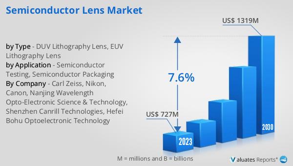
The global market for semiconductor lenses was valued at $849 million in 2024, and it is anticipated to grow significantly, reaching an estimated size of $1,410 million by 2031. This growth trajectory represents a compound annual growth rate (CAGR) of 7.6% over the forecast period. This upward trend is indicative of the increasing demand for semiconductor lenses, driven by the rapid advancements in technology and the growing need for high-performance electronic devices. The market's expansion is fueled by the continuous innovation in semiconductor manufacturing processes, where lenses play a crucial role in achieving the precision and accuracy required for modern microchips. As the semiconductor industry evolves, the demand for more efficient and precise lenses is expected to grow, making the Global Semiconductor Lens Market a dynamic and rapidly developing sector. The market is characterized by continuous innovation and technological advancements, as manufacturers strive to meet the ever-increasing demands of the electronics industry. This growth is not only a reflection of the increasing demand for advanced electronic devices but also highlights the critical role that semiconductor lenses play in the production of these devices. As the industry continues to push the boundaries of what is possible, the demand for advanced lithography lenses will only increase, making them a key focus for research and development efforts.
| Report Metric | Details |
| Report Name | Semiconductor Lens Market |
| Accounted market size in year | US$ 849 million |
| Forecasted market size in 2031 | US$ 1410 million |
| CAGR | 7.6% |
| Base Year | year |
| Forecasted years | 2025 - 2031 |
| by Type |
|
| by Application |
|
| Production by Region |
|
| Consumption by Region |
|
| By Company | Carl Zeiss, Nikon, Canon, Nanjing Wavelength Opto-Electronic Science & Technology, Shenzhen Canrill Technologies, Hefei Bohu Optoelectronic Technology |
| Forecast units | USD million in value |
| Report coverage | Revenue and volume forecast, company share, competitive landscape, growth factors and trends |


