What is Global Lithography Lens Market?
The Global Lithography Lens Market is a crucial segment within the semiconductor and electronics industry, focusing on the production and development of lenses used in lithography systems. Lithography is a pivotal process in semiconductor manufacturing, where patterns are transferred onto silicon wafers to create integrated circuits. The lenses used in this process are highly specialized, designed to focus light or other radiation onto the wafer with extreme precision. These lenses are integral to the photolithography process, which is essential for producing the tiny, intricate patterns required in modern electronic devices. As technology advances, the demand for more sophisticated and precise lithography lenses increases, driving innovation and growth in this market. The market encompasses various types of lenses, including those used in Deep Ultraviolet (DUV) and Extreme Ultraviolet (EUV) lithography, each catering to different technological needs and manufacturing processes. The growth of the global lithography lens market is fueled by the continuous evolution of semiconductor technology, the increasing complexity of electronic devices, and the relentless pursuit of smaller, more efficient components. As a result, the market is characterized by rapid technological advancements, significant research and development investments, and a competitive landscape with key players striving to enhance lens performance and reduce production costs.
DUV Lithography Lens, EUV Lithography Lens in the Global Lithography Lens Market:
In the realm of the Global Lithography Lens Market, two primary types of lenses stand out: Deep Ultraviolet (DUV) Lithography Lenses and Extreme Ultraviolet (EUV) Lithography Lenses. DUV lithography lenses operate at wavelengths typically around 193 nanometers and are widely used in the semiconductor industry for producing microchips. These lenses are crucial for the photolithography process, where they focus ultraviolet light to etch intricate patterns onto silicon wafers. The precision and efficiency of DUV lenses make them indispensable for manufacturing a wide range of electronic components, from microprocessors to memory chips. As the demand for smaller and more powerful electronic devices grows, the need for advanced DUV lithography lenses continues to rise, driving innovation and development in this segment of the market. On the other hand, EUV lithography lenses represent the cutting edge of lithography technology. Operating at a much shorter wavelength of 13.5 nanometers, EUV lenses enable the production of even smaller and more complex semiconductor patterns. This technology is essential for the next generation of microchips, which require incredibly fine features to meet the demands of modern computing and electronic devices. The development and deployment of EUV lithography lenses are more challenging and costly compared to DUV lenses, but they offer unparalleled precision and efficiency. As the semiconductor industry pushes the boundaries of miniaturization and performance, EUV lithography lenses are becoming increasingly important. The transition from DUV to EUV lithography is a significant milestone in the evolution of semiconductor manufacturing, and it underscores the critical role that lithography lenses play in this process. Both DUV and EUV lithography lenses are at the forefront of technological advancement, driving the growth and transformation of the Global Lithography Lens Market. As manufacturers strive to meet the ever-increasing demands for smaller, faster, and more efficient electronic devices, the importance of these lenses cannot be overstated. The continuous development and refinement of lithography lens technology are essential for the future of the semiconductor industry and the broader electronics market.
Semiconductor Manufacturing, Optoelectronic components, Others in the Global Lithography Lens Market:
The Global Lithography Lens Market finds its applications in several key areas, including semiconductor manufacturing, optoelectronic components, and other industries. In semiconductor manufacturing, lithography lenses are indispensable tools used to project circuit patterns onto silicon wafers. This process is fundamental to the production of integrated circuits, which are the building blocks of all electronic devices. The precision and accuracy of lithography lenses directly impact the performance and efficiency of the semiconductors produced. As the demand for smaller, more powerful, and energy-efficient electronic devices continues to grow, the need for advanced lithography lenses becomes even more critical. These lenses enable manufacturers to produce chips with smaller features and higher densities, which are essential for modern computing, telecommunications, and consumer electronics. In the realm of optoelectronic components, lithography lenses play a vital role in the production of devices that combine optical and electronic functions. These components are used in a wide range of applications, from fiber-optic communication systems to advanced imaging technologies. The precision and versatility of lithography lenses allow for the creation of complex optical patterns and structures, which are essential for the performance and functionality of optoelectronic devices. As the demand for high-speed data transmission and advanced imaging solutions continues to rise, the importance of lithography lenses in this sector cannot be overstated. Beyond semiconductor manufacturing and optoelectronic components, the Global Lithography Lens Market also serves other industries that require precise patterning and imaging capabilities. This includes fields such as biotechnology, where lithography lenses are used in the production of microfluidic devices and lab-on-a-chip technologies. These applications require the ability to create intricate patterns and structures on a microscopic scale, which is made possible by the advanced capabilities of lithography lenses. Additionally, the market serves industries involved in the production of advanced sensors, displays, and other electronic components that require precise patterning and imaging. The versatility and precision of lithography lenses make them indispensable tools in a wide range of applications, driving innovation and growth across multiple industries. As technology continues to evolve and the demand for advanced electronic devices and components increases, the Global Lithography Lens Market is poised for continued growth and expansion.
Global Lithography Lens Market Outlook:
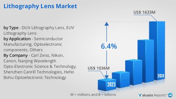
The global market for lithography lenses was valued at approximately $1,126 million in 2024, and it is anticipated to grow significantly, reaching an estimated $1,727 million by 2031. This growth trajectory represents a compound annual growth rate (CAGR) of 6.4% over the forecast period. This upward trend underscores the increasing demand for advanced lithography lenses, driven by the rapid advancements in semiconductor technology and the growing complexity of electronic devices. As the industry continues to push the boundaries of miniaturization and performance, the need for more precise and efficient lithography lenses becomes paramount. The market's expansion is fueled by the relentless pursuit of smaller, faster, and more efficient electronic components, which are essential for modern computing, telecommunications, and consumer electronics. The transition from traditional lithography techniques to more advanced methods, such as DUV and EUV lithography, further accelerates the market's growth. These advanced technologies enable the production of smaller and more complex semiconductor patterns, meeting the demands of the next generation of electronic devices. As a result, the global lithography lens market is characterized by rapid technological advancements, significant research and development investments, and a competitive landscape with key players striving to enhance lens performance and reduce production costs. The continuous development and refinement of lithography lens technology are essential for the future of the semiconductor industry and the broader electronics market.
| Report Metric | Details |
| Report Name | Lithography Lens Market |
| Accounted market size in year | US$ 1126 million |
| Forecasted market size in 2031 | US$ 1727 million |
| CAGR | 6.4% |
| Base Year | year |
| Forecasted years | 2025 - 2031 |
| by Type |
|
| by Application |
|
| Production by Region |
|
| Consumption by Region |
|
| By Company | Carl Zeiss, Nikon, Canon, Nanjing Wavelength Opto-Electronic Science & Technology, Shenzhen Canrill Technologies, Hefei Bohu Optoelectronic Technology |
| Forecast units | USD million in value |
| Report coverage | Revenue and volume forecast, company share, competitive landscape, growth factors and trends |


