What is Global Laser Direct Writing Lithography Lens Market?
The Global Laser Direct Writing Lithography Lens Market is a specialized segment within the broader lithography equipment industry, focusing on the development and production of lenses used in laser direct writing lithography systems. These systems are pivotal in the semiconductor manufacturing process, where they enable the precise patterning of micro and nano-scale features on substrates. The market is driven by the increasing demand for miniaturized electronic devices, which require advanced lithography techniques to produce smaller and more efficient components. Laser direct writing lithography offers several advantages, including high resolution, flexibility, and the ability to create complex patterns without the need for masks, making it an attractive option for manufacturers. The market is characterized by continuous technological advancements, as companies strive to improve the performance and capabilities of their lenses to meet the evolving needs of the semiconductor industry. Additionally, the market is influenced by factors such as the growing adoption of IoT devices, advancements in 5G technology, and the increasing complexity of integrated circuits. As a result, the Global Laser Direct Writing Lithography Lens Market is poised for significant growth, driven by the ongoing demand for cutting-edge semiconductor manufacturing solutions.
DUV Lithography Lens, EUV Lithography Lens in the Global Laser Direct Writing Lithography Lens Market:
Deep Ultraviolet (DUV) Lithography Lens and Extreme Ultraviolet (EUV) Lithography Lens are two critical components in the Global Laser Direct Writing Lithography Lens Market, each serving distinct roles in the semiconductor manufacturing process. DUV lithography lenses operate in the deep ultraviolet spectrum, typically around 193 nanometers, and are widely used in the production of integrated circuits. These lenses are essential for achieving the high resolution required to produce the intricate patterns found in modern semiconductor devices. DUV lithography has been the workhorse of the semiconductor industry for many years, enabling the production of smaller and more powerful chips. However, as the demand for even smaller feature sizes continues to grow, the limitations of DUV lithography have become more apparent, leading to the development of EUV lithography. EUV lithography lenses operate at a much shorter wavelength of 13.5 nanometers, allowing for even higher resolution and the production of smaller features. This technology is crucial for the continued advancement of Moore's Law, which predicts the doubling of transistors on a chip approximately every two years. EUV lithography is particularly important for the production of advanced nodes, such as 7nm and below, where traditional DUV lithography struggles to achieve the necessary resolution. The transition from DUV to EUV lithography represents a significant technological leap, requiring substantial investment in new equipment and processes. Despite the challenges, the adoption of EUV lithography is accelerating, driven by the need for more powerful and efficient semiconductor devices. Both DUV and EUV lithography lenses are integral to the Global Laser Direct Writing Lithography Lens Market, as they enable the production of the next generation of electronic devices. As the semiconductor industry continues to evolve, the demand for advanced lithography solutions will only increase, driving further innovation and growth in this market.
PCB Circuit Board Printing, Solder Mask Ink Printing, IC Carrier Board Printing, Others in the Global Laser Direct Writing Lithography Lens Market:
The Global Laser Direct Writing Lithography Lens Market plays a crucial role in various applications, including PCB circuit board printing, solder mask ink printing, IC carrier board printing, and others. In PCB circuit board printing, laser direct writing lithography lenses are used to create precise patterns on the circuit boards, which are essential for the functionality of electronic devices. The high resolution and accuracy of these lenses allow for the production of complex circuit designs, enabling the development of smaller and more efficient electronic components. This is particularly important in the era of miniaturization, where the demand for compact and powerful devices is ever-increasing. In solder mask ink printing, laser direct writing lithography lenses are used to apply a protective layer over the circuit board, preventing short circuits and protecting the board from environmental damage. The precision of these lenses ensures that the solder mask is applied accurately, covering only the necessary areas and leaving the contact points exposed for soldering. This is critical for the reliability and longevity of electronic devices, as any errors in the application of the solder mask can lead to malfunctions or failures. In IC carrier board printing, laser direct writing lithography lenses are used to create the intricate patterns required for the interconnection of integrated circuits. These lenses enable the production of high-density interconnects, which are essential for the performance and efficiency of modern electronic devices. The ability to produce complex patterns with high precision is a key advantage of laser direct writing lithography, making it an ideal solution for the production of IC carrier boards. Beyond these specific applications, the Global Laser Direct Writing Lithography Lens Market is also used in other areas, such as the production of microelectromechanical systems (MEMS), photonic devices, and advanced packaging solutions. The versatility and precision of laser direct writing lithography lenses make them an invaluable tool in the manufacturing of a wide range of electronic components, driving innovation and growth in the electronics industry.
Global Laser Direct Writing Lithography Lens Market Outlook:
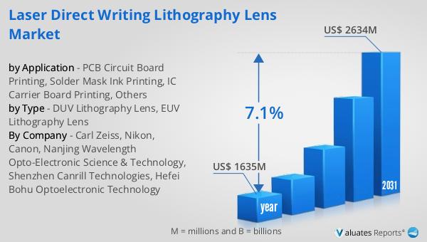
The global market for Laser Direct Writing Lithography Lens was valued at $1,635 million in 2024 and is anticipated to expand to a revised size of $2,634 million by 2031, reflecting a compound annual growth rate (CAGR) of 7.1% over the forecast period. This growth trajectory underscores the increasing demand for advanced lithography solutions in the semiconductor industry, driven by the need for smaller, more efficient electronic devices. The market's expansion is fueled by several factors, including the ongoing miniaturization of electronic components, advancements in 5G technology, and the proliferation of IoT devices. As the complexity of integrated circuits continues to rise, the demand for high-resolution lithography lenses capable of producing intricate patterns with precision is expected to grow. The transition from DUV to EUV lithography is also a significant driver of market growth, as manufacturers invest in new equipment and processes to meet the demands of advanced semiconductor nodes. Despite the challenges associated with this transition, the adoption of EUV lithography is accelerating, further contributing to the market's expansion. Overall, the Global Laser Direct Writing Lithography Lens Market is poised for significant growth, driven by the ongoing demand for cutting-edge semiconductor manufacturing solutions and the continuous evolution of the electronics industry.
| Report Metric | Details |
| Report Name | Laser Direct Writing Lithography Lens Market |
| Accounted market size in year | US$ 1635 million |
| Forecasted market size in 2031 | US$ 2634 million |
| CAGR | 7.1% |
| Base Year | year |
| Forecasted years | 2025 - 2031 |
| by Type |
|
| by Application |
|
| Production by Region |
|
| Consumption by Region |
|
| By Company | Carl Zeiss, Nikon, Canon, Nanjing Wavelength Opto-Electronic Science & Technology, Shenzhen Canrill Technologies, Hefei Bohu Optoelectronic Technology |
| Forecast units | USD million in value |
| Report coverage | Revenue and volume forecast, company share, competitive landscape, growth factors and trends |


