What is Global Semiconductor Cleaning Agents Market?
The Global Semiconductor Cleaning Agents Market is a crucial segment within the semiconductor industry, focusing on the production and distribution of cleaning agents used in semiconductor manufacturing. These agents are essential for maintaining the purity and functionality of semiconductor devices, which are integral to a wide range of electronic products. The market encompasses various types of cleaning agents, including those used for removing impurities, residues, and contaminants from semiconductor wafers during different stages of production. The demand for these cleaning agents is driven by the increasing complexity and miniaturization of semiconductor devices, which require highly precise and effective cleaning solutions to ensure optimal performance. As technology advances, the need for more sophisticated cleaning agents grows, making this market a vital component of the semiconductor supply chain. The market is characterized by continuous innovation and development, as manufacturers strive to meet the evolving needs of the semiconductor industry. This dynamic environment fosters competition and collaboration among key players, leading to the introduction of new and improved cleaning solutions that enhance the efficiency and reliability of semiconductor manufacturing processes.
Post-etching Cleaning Solutions, Photoresist Cleaning Solutions, Post CMP Cleaning Solutions in the Global Semiconductor Cleaning Agents Market:
Post-etching cleaning solutions, photoresist cleaning solutions, and post-CMP (Chemical Mechanical Planarization) cleaning solutions are integral components of the Global Semiconductor Cleaning Agents Market. Post-etching cleaning solutions are designed to remove residues and contaminants left on semiconductor wafers after the etching process. Etching is a critical step in semiconductor manufacturing, where specific patterns are created on the wafer surface. However, this process often leaves behind unwanted residues that can affect the performance of the final product. Post-etching cleaning solutions effectively eliminate these residues, ensuring the wafer's surface is clean and ready for subsequent processing steps. These solutions are formulated to target specific contaminants, such as polymers and metal residues, without damaging the delicate structures on the wafer. Photoresist cleaning solutions, on the other hand, are used to remove photoresist materials applied during the photolithography process. Photolithography is a technique used to transfer patterns onto the semiconductor wafer, and photoresists are light-sensitive materials that help define these patterns. After the desired pattern is created, the remaining photoresist must be removed to prevent interference with further processing. Photoresist cleaning solutions are specially formulated to dissolve and remove these materials without harming the underlying wafer. They play a crucial role in maintaining the integrity of the patterns and ensuring the accuracy of the semiconductor devices. Post-CMP cleaning solutions are used after the Chemical Mechanical Planarization process, which is employed to smooth and flatten the wafer surface. CMP is essential for achieving the required planarity and uniformity of the wafer, but it can leave behind abrasive particles and residues. Post-CMP cleaning solutions are designed to remove these particles and residues, ensuring a clean and smooth surface for subsequent processing. These solutions are formulated to be gentle on the wafer while effectively removing contaminants, preventing defects and improving the yield of semiconductor devices. The development of these cleaning solutions involves extensive research and testing to ensure compatibility with various materials and processes used in semiconductor manufacturing. Manufacturers continuously innovate to create more effective and environmentally friendly cleaning agents, addressing the industry's growing demand for sustainable solutions. The Global Semiconductor Cleaning Agents Market is driven by the increasing complexity of semiconductor devices, which require precise and efficient cleaning solutions to maintain their performance and reliability. As the industry continues to evolve, the demand for advanced cleaning agents is expected to grow, making this market a vital component of the semiconductor supply chain.
200mm Process, 300mm Process, Others in the Global Semiconductor Cleaning Agents Market:
The usage of Global Semiconductor Cleaning Agents Market in the 200mm process, 300mm process, and other semiconductor manufacturing processes highlights the versatility and importance of these cleaning agents. The 200mm process refers to the production of semiconductor wafers with a diameter of 200 millimeters. This process is widely used in the manufacturing of various electronic components, including microcontrollers, sensors, and power devices. Cleaning agents play a crucial role in the 200mm process by ensuring the removal of contaminants and residues that can affect the performance and reliability of the final products. The cleaning agents used in this process are formulated to address the specific challenges associated with 200mm wafers, such as the removal of metal residues and organic contaminants. The 300mm process, on the other hand, involves the production of larger semiconductor wafers with a diameter of 300 millimeters. This process is commonly used in the manufacturing of advanced semiconductor devices, such as microprocessors and memory chips. The larger wafer size allows for the production of more devices per wafer, increasing efficiency and reducing costs. However, the 300mm process also presents unique challenges, as the larger surface area requires more precise and effective cleaning solutions. Cleaning agents used in the 300mm process are designed to provide thorough cleaning while minimizing the risk of damage to the wafer. They are formulated to remove a wide range of contaminants, including particles, residues, and films, ensuring the highest level of cleanliness and performance. In addition to the 200mm and 300mm processes, semiconductor cleaning agents are also used in other manufacturing processes, such as the production of compound semiconductors and MEMS (Micro-Electro-Mechanical Systems) devices. These processes often involve unique materials and structures, requiring specialized cleaning solutions to address specific challenges. The versatility of semiconductor cleaning agents allows them to be adapted to various processes, ensuring the highest level of cleanliness and performance across different applications. The development of cleaning agents for these processes involves extensive research and testing to ensure compatibility with different materials and manufacturing techniques. Manufacturers continuously innovate to create more effective and environmentally friendly cleaning solutions, addressing the industry's growing demand for sustainable and efficient processes. The Global Semiconductor Cleaning Agents Market is driven by the increasing complexity and diversity of semiconductor manufacturing processes, which require precise and efficient cleaning solutions to maintain the performance and reliability of semiconductor devices. As the industry continues to evolve, the demand for advanced cleaning agents is expected to grow, making this market a vital component of the semiconductor supply chain.
Global Semiconductor Cleaning Agents Market Outlook:
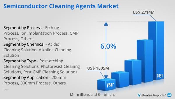
The global market for semiconductor cleaning agents was valued at $1,805 million in 2024, and it is anticipated to expand to a revised size of $2,714 million by 2031, reflecting a compound annual growth rate (CAGR) of 6.0% over the forecast period. This growth trajectory underscores the increasing demand for semiconductor cleaning agents, driven by the rapid advancements in semiconductor technology and the growing complexity of semiconductor devices. As the industry continues to innovate and develop more sophisticated electronic components, the need for effective and efficient cleaning solutions becomes paramount. Semiconductor cleaning agents play a critical role in ensuring the purity and functionality of semiconductor devices, which are integral to a wide range of electronic products. The market's growth is also fueled by the rising adoption of advanced manufacturing processes, such as the 300mm process, which requires more precise and effective cleaning solutions. Additionally, the increasing focus on sustainability and environmental responsibility is driving the development of more environmentally friendly cleaning agents, further contributing to the market's expansion. As the semiconductor industry continues to evolve, the demand for advanced cleaning agents is expected to grow, making this market a vital component of the semiconductor supply chain.
| Report Metric | Details |
| Report Name | Semiconductor Cleaning Agents Market |
| Accounted market size in year | US$ 1805 million |
| Forecasted market size in 2031 | US$ 2714 million |
| CAGR | 6.0% |
| Base Year | year |
| Forecasted years | 2025 - 2031 |
| Segment by Type |
|
| Segment by Chemical |
|
| Segment by Process |
|
| Segment by Application |
|
| Production by Region |
|
| Consumption by Region |
|
| By Company | Entegris, Qnity (DuPont), Merck (Versum Materials), JSR Corporation, Mitsubishi Gas Chemical, Dongjin Semichem, FUJIFILM, BASF, LG Chem, Tokyo Ohka Kogyo, ENF Tech, Nagase, Kanto Chemical, Avantor, Solexir Technoloy, Technic Inc, Anji Microelectronics Technology, Jiangyin Jianghua Micro-electronic Materials Co., Ltd, San Fu Chemical Co., Ltd |
| Forecast units | USD million in value |
| Report coverage | Revenue and volume forecast, company share, competitive landscape, growth factors and trends |