What is Global Cutting-Edge Processes Wafer Foundry Market?
The Global Cutting-Edge Processes Wafer Foundry Market is a specialized sector within the semiconductor industry that focuses on the production of advanced semiconductor wafers. These wafers are the foundational building blocks for a wide range of electronic devices, from smartphones to high-performance computing systems. The term "cutting-edge processes" refers to the most advanced manufacturing techniques used to produce these wafers, often involving the latest technology nodes such as 5nm, 3nm, and even smaller. These processes are crucial for enhancing the performance, efficiency, and capabilities of electronic devices. Foundries, which are specialized manufacturing plants, play a pivotal role in this market by providing the infrastructure and expertise needed to produce these advanced wafers. The demand for cutting-edge processes is driven by the rapid evolution of technology and the increasing need for more powerful and efficient electronic devices. As industries such as telecommunications, computing, and consumer electronics continue to grow, the importance of the Global Cutting-Edge Processes Wafer Foundry Market is expected to increase, making it a critical component of the global technology landscape.
in the Global Cutting-Edge Processes Wafer Foundry Market:
In the Global Cutting-Edge Processes Wafer Foundry Market, various types of wafers are utilized by different customers, each catering to specific technological needs and applications. One of the primary types is the logic wafer, which is essential for the functioning of processors and integrated circuits. These wafers are crucial for devices that require high-speed processing and efficient power consumption, such as smartphones and computers. Another significant type is the memory wafer, used in the production of DRAM and NAND flash memory. These are vital for data storage solutions in a wide array of devices, from personal gadgets to large-scale data centers. Analog wafers are also a key component, used in devices that require the conversion of real-world signals into digital data, such as sensors and communication devices. Additionally, there are specialty wafers designed for specific applications like radio frequency (RF) and power management. RF wafers are critical for wireless communication technologies, enabling devices to transmit and receive signals effectively. Power management wafers, on the other hand, are used in devices that require efficient energy consumption and heat dissipation, such as electric vehicles and renewable energy systems. Each type of wafer is tailored to meet the unique demands of its application, ensuring optimal performance and efficiency. The choice of wafer type is influenced by factors such as the intended application, performance requirements, and cost considerations. As technology continues to advance, the diversity and specialization of wafer types in the Global Cutting-Edge Processes Wafer Foundry Market are expected to expand, catering to the evolving needs of various industries. This diversity not only highlights the complexity of the market but also underscores the importance of innovation and adaptability in meeting the demands of modern technology.
High Performance Computing (HPC), Smartphone, Computer, Others in the Global Cutting-Edge Processes Wafer Foundry Market:
The Global Cutting-Edge Processes Wafer Foundry Market plays a crucial role in several key areas, including High Performance Computing (HPC), smartphones, computers, and other electronic devices. In the realm of High Performance Computing, advanced wafers are essential for creating powerful processors that can handle complex computations and large data sets. These wafers enable the development of supercomputers and data centers that are vital for scientific research, financial modeling, and artificial intelligence applications. In the smartphone industry, cutting-edge wafers are used to produce processors that offer high speed, energy efficiency, and enhanced capabilities. This is crucial for meeting the demands of modern smartphones, which require advanced features such as high-resolution cameras, augmented reality, and seamless connectivity. For computers, both personal and enterprise-level, advanced wafers are used to manufacture CPUs and GPUs that deliver superior performance and efficiency. This is important for applications ranging from everyday computing tasks to intensive gaming and professional software. Beyond these specific areas, the Global Cutting-Edge Processes Wafer Foundry Market also supports a wide range of other applications, including automotive electronics, Internet of Things (IoT) devices, and industrial automation. In each of these areas, the ability to produce advanced wafers is critical for driving innovation and meeting the growing demands of technology. As the market continues to evolve, the role of cutting-edge processes in enabling new and improved electronic devices is expected to become even more significant.
Global Cutting-Edge Processes Wafer Foundry Market Outlook:
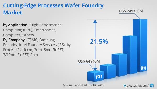
The global market for Cutting-Edge Processes Wafer Foundry was valued at approximately $64.94 billion in 2024, and it is anticipated to grow significantly, reaching an estimated size of $249.35 billion by 2031. This impressive growth trajectory represents a compound annual growth rate (CAGR) of 21.5% over the forecast period. This rapid expansion is indicative of the increasing demand for advanced semiconductor wafers across various industries. The growth is driven by the continuous advancements in technology and the rising need for more powerful and efficient electronic devices. As industries such as telecommunications, computing, and consumer electronics continue to evolve, the demand for cutting-edge processes in wafer foundries is expected to rise. This growth also reflects the critical role that these advanced processes play in enabling the development of next-generation electronic devices. The market's expansion is a testament to the importance of innovation and technological advancement in the semiconductor industry. As the market continues to grow, it is likely to have a significant impact on the global technology landscape, driving further advancements and shaping the future of electronic devices.
| Report Metric | Details |
| Report Name | Cutting-Edge Processes Wafer Foundry Market |
| Accounted market size in year | US$ 64940 million |
| Forecasted market size in 2031 | US$ 249350 million |
| CAGR | 21.5% |
| Base Year | year |
| Forecasted years | 2025 - 2031 |
| by Application |
|
| Production by Region |
|
| Consumption by Region |
|
| By Company | TSMC, Samsung Foundry, Intel Foundry Services (IFS), by Process Platform, 3nm, 5nm FinFET, 7/10nm FinFET, 2nm |
| Forecast units | USD million in value |
| Report coverage | Revenue and volume forecast, company share, competitive landscape, growth factors and trends |


