What is Global Advanced Process Node Wafer Foundry Market?
The Global Advanced Process Node Wafer Foundry Market refers to the industry involved in the production of semiconductor wafers using advanced process nodes. These process nodes are essentially the technology generations used in semiconductor manufacturing, with smaller nodes indicating more advanced technology. As technology progresses, the demand for smaller, more efficient, and powerful semiconductor devices increases, driving the need for advanced process nodes. Foundries, which are specialized manufacturing plants, play a crucial role in this market by fabricating chips for various applications, including consumer electronics, automotive, and telecommunications. The market is characterized by rapid technological advancements, significant capital investments, and a competitive landscape dominated by a few key players. These foundries are essential for producing the cutting-edge chips that power modern electronic devices, making them a critical component of the global technology supply chain. As industries continue to innovate and demand more sophisticated electronic components, the Global Advanced Process Node Wafer Foundry Market is poised for continued growth and evolution.
in the Global Advanced Process Node Wafer Foundry Market:
The Global Advanced Process Node Wafer Foundry Market is diverse, catering to a wide range of customer needs through various types of process nodes. These nodes are defined by their size, measured in nanometers (nm), with smaller numbers indicating more advanced technology. The most common types include 7nm, 5nm, and 3nm nodes, each offering different benefits and challenges. The 7nm node, for instance, is widely used for its balance of performance and cost-effectiveness, making it popular among smartphone manufacturers and high-performance computing (HPC) applications. It allows for increased transistor density, which enhances processing power while reducing energy consumption. The 5nm node takes this a step further, offering even greater efficiency and performance, which is crucial for applications requiring high computational power, such as artificial intelligence and machine learning. The 3nm node, although still emerging, promises to revolutionize the industry with its unprecedented performance capabilities, enabling the development of even more powerful and efficient devices. Customers in this market range from consumer electronics companies to automotive manufacturers, each with unique requirements that drive the demand for specific process nodes. For instance, smartphone manufacturers prioritize energy efficiency and compact design, while automotive companies focus on reliability and performance. The diversity of applications and customer needs ensures that the Global Advanced Process Node Wafer Foundry Market remains dynamic and adaptable, continuously evolving to meet the demands of a rapidly changing technological landscape.
High Performance Computing (HPC), Smartphone, Wearable and IoT Devices, Automotive, Others in the Global Advanced Process Node Wafer Foundry Market:
The usage of the Global Advanced Process Node Wafer Foundry Market spans several key areas, each with distinct requirements and challenges. In High Performance Computing (HPC), advanced process nodes are crucial for developing powerful processors that can handle complex computations and large data sets. These nodes enable the creation of chips with higher transistor densities, which translates to faster processing speeds and improved energy efficiency. This is essential for applications such as scientific research, financial modeling, and data analytics, where performance and speed are critical. In the smartphone industry, advanced process nodes are used to produce chips that offer a balance of performance and power efficiency, enabling longer battery life and enhanced functionality in increasingly compact devices. Wearable and IoT devices also benefit from these nodes, as they require small, energy-efficient chips to function effectively in a wide range of environments. In the automotive sector, advanced process nodes are used to develop chips that power everything from infotainment systems to advanced driver-assistance systems (ADAS), where reliability and performance are paramount. Other areas, such as telecommunications and consumer electronics, also rely on advanced process nodes to produce the cutting-edge chips that drive innovation and enhance user experiences. The versatility and adaptability of advanced process nodes make them indispensable across a wide range of industries, driving the growth and evolution of the Global Advanced Process Node Wafer Foundry Market.
Global Advanced Process Node Wafer Foundry Market Outlook:
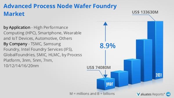
The global market for Advanced Process Node Wafer Foundry was valued at $74,080 million in 2024 and is anticipated to expand to a revised size of $133,630 million by 2031, reflecting a compound annual growth rate (CAGR) of 8.9% over the forecast period. This growth is driven by the increasing demand for advanced semiconductor devices across various industries, including consumer electronics, automotive, and telecommunications. As technology continues to evolve, the need for smaller, more efficient, and powerful chips becomes more pronounced, fueling the demand for advanced process nodes. Foundries play a critical role in this market by providing the manufacturing capabilities necessary to produce these cutting-edge chips. The competitive landscape is dominated by a few key players, each investing heavily in research and development to stay ahead of the curve. As industries continue to innovate and demand more sophisticated electronic components, the Global Advanced Process Node Wafer Foundry Market is poised for continued growth and evolution. The market's expansion is a testament to the importance of advanced process nodes in driving technological progress and meeting the ever-increasing demands of modern electronic devices.
| Report Metric | Details |
| Report Name | Advanced Process Node Wafer Foundry Market |
| Accounted market size in year | US$ 74080 million |
| Forecasted market size in 2031 | US$ 133630 million |
| CAGR | 8.9% |
| Base Year | year |
| Forecasted years | 2025 - 2031 |
| by Application |
|
| Production by Region |
|
| Consumption by Region |
|
| By Company | TSMC, Samsung Foundry, Intel Foundry Services (IFS), GlobalFoundries, SMIC, HLMC, by Process Platform, 3nm, 5nm, 7nm, 10/12/14/16/20nm |
| Forecast units | USD million in value |
| Report coverage | Revenue and volume forecast, company share, competitive landscape, growth factors and trends |


