What is Global Mature Process Node Wafer Foundry Market?
The Global Mature Process Node Wafer Foundry Market refers to the segment of the semiconductor industry that focuses on the production of wafers using mature process nodes. These process nodes are typically older technology nodes, such as 28nm, 40nm, 65nm, and above, which are not the latest in terms of miniaturization but are still widely used due to their cost-effectiveness and reliability. These mature nodes are crucial for manufacturing a wide range of semiconductor devices that do not require the cutting-edge performance of the latest nodes. The market is driven by the demand for these nodes in various applications, including consumer electronics, automotive, industrial, and IoT devices. As technology advances, the need for mature process nodes remains strong because they offer a balance between performance and cost, making them ideal for products where the latest technology is not necessary. The foundries that specialize in these nodes provide essential services to companies that design chips but do not have the capability to manufacture them in-house. This market is characterized by its stability and steady growth, as mature nodes continue to be relevant in many sectors.
in the Global Mature Process Node Wafer Foundry Market:
The Global Mature Process Node Wafer Foundry Market serves a diverse range of customers, each with specific needs that are met by different types of mature process nodes. These nodes are categorized based on their technology, such as 28nm, 40nm, 65nm, and older nodes like 90nm and 130nm. Each type of node offers unique advantages that cater to various applications. For instance, the 28nm node is popular for its balance between performance and power efficiency, making it suitable for mobile and consumer electronics. It provides a good compromise between cost and capability, allowing manufacturers to produce high-performance chips without the expense of the latest technology. On the other hand, the 40nm node is often used in applications where cost is a more significant concern than performance, such as in certain consumer electronics and industrial applications. This node is known for its reliability and lower production costs, which are crucial for products that need to be affordable yet functional. The 65nm node is another widely used type, particularly in automotive and industrial sectors. Its robustness and proven track record make it ideal for applications that require durability and long-term reliability. Automotive electronics, for example, benefit from the 65nm node's ability to withstand harsh conditions and deliver consistent performance over time. Similarly, industrial applications that demand high reliability and longevity often rely on this node. Older nodes like 90nm and 130nm are still in use for specific applications where the latest technology is not necessary. These nodes are particularly cost-effective and are used in products where performance requirements are minimal, such as certain types of sensors and basic electronic components. They offer a low-cost solution for manufacturers looking to produce large volumes of simple devices. The choice of node depends largely on the specific requirements of the application, including factors like power consumption, performance, cost, and reliability. Customers in the Global Mature Process Node Wafer Foundry Market select the appropriate node based on these criteria, ensuring that their products meet the necessary specifications while remaining economically viable. This diversity in node types allows the market to cater to a wide range of industries and applications, each with its unique demands and challenges.
Consumer & Mobile, Internet of Things (IoT), Automotive, Industrial, Others in the Global Mature Process Node Wafer Foundry Market:
The Global Mature Process Node Wafer Foundry Market plays a crucial role in several key areas, including Consumer & Mobile, Internet of Things (IoT), Automotive, Industrial, and others. In the Consumer & Mobile sector, mature process nodes are essential for manufacturing chips used in smartphones, tablets, and other consumer electronics. These nodes provide a cost-effective solution for producing high-performance chips that power a wide range of devices. The balance between performance and cost is particularly important in this sector, where manufacturers need to deliver cutting-edge technology at competitive prices. In the Internet of Things (IoT) domain, mature process nodes are used to produce chips for a variety of connected devices. These nodes offer the power efficiency and reliability needed for IoT applications, where devices often operate on battery power and require long-term stability. The ability to produce low-cost, energy-efficient chips is crucial for the widespread adoption of IoT technology, making mature nodes an ideal choice for this market. The Automotive sector also relies heavily on mature process nodes for producing chips used in various electronic systems within vehicles. These nodes provide the durability and reliability needed to withstand the harsh conditions of automotive environments. From engine control units to infotainment systems, mature nodes ensure that automotive electronics perform consistently and reliably over the lifespan of the vehicle. In the Industrial sector, mature process nodes are used in a wide range of applications, from factory automation to energy management systems. The robustness and long-term reliability of these nodes make them suitable for industrial environments, where equipment must operate continuously and withstand challenging conditions. The ability to produce cost-effective, reliable chips is essential for industrial applications, where downtime can be costly and disruptive. Other areas that benefit from the Global Mature Process Node Wafer Foundry Market include telecommunications, healthcare, and aerospace. In telecommunications, mature nodes are used to produce chips for networking equipment and communication devices, where reliability and performance are critical. In healthcare, these nodes are used in medical devices and equipment, where precision and reliability are paramount. In aerospace, mature nodes provide the durability and performance needed for electronic systems used in aircraft and spacecraft. Overall, the Global Mature Process Node Wafer Foundry Market supports a wide range of industries and applications, each with its unique requirements and challenges. The ability to produce cost-effective, reliable chips using mature process nodes is essential for the continued growth and development of these sectors.
Global Mature Process Node Wafer Foundry Market Outlook:
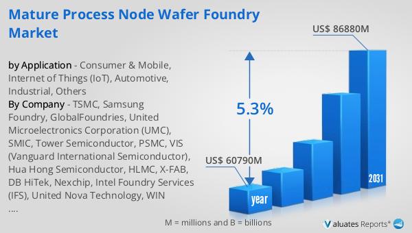
The global market for Mature Process Node Wafer Foundry was valued at $60,790 million in 2024 and is anticipated to expand to a revised size of $86,880 million by 2031, reflecting a compound annual growth rate (CAGR) of 5.3% during the forecast period. This growth trajectory underscores the enduring relevance and demand for mature process nodes in the semiconductor industry. Despite the rapid advancements in technology and the push towards smaller, more advanced nodes, mature process nodes continue to hold significant importance due to their cost-effectiveness and reliability. These nodes are integral to a wide array of applications across various sectors, including consumer electronics, automotive, industrial, and IoT devices. The steady growth of this market is driven by the need for affordable and reliable semiconductor solutions that do not necessarily require the latest technology. As industries continue to evolve and expand, the demand for mature process nodes is expected to remain strong, supporting the production of a diverse range of electronic devices. The projected growth of the Global Mature Process Node Wafer Foundry Market highlights the critical role these nodes play in the semiconductor industry, providing essential solutions for manufacturers and designers worldwide.
| Report Metric | Details |
| Report Name | Mature Process Node Wafer Foundry Market |
| Accounted market size in year | US$ 60790 million |
| Forecasted market size in 2031 | US$ 86880 million |
| CAGR | 5.3% |
| Base Year | year |
| Forecasted years | 2025 - 2031 |
| by Application |
|
| Production by Region |
|
| Consumption by Region |
|
| By Company | TSMC, Samsung Foundry, GlobalFoundries, United Microelectronics Corporation (UMC), SMIC, Tower Semiconductor, PSMC, VIS (Vanguard International Semiconductor), Hua Hong Semiconductor, HLMC, X-FAB, DB HiTek, Nexchip, Intel Foundry Services (IFS), United Nova Technology, WIN Semiconductors Corp., Wuhan Xinxin Semiconductor Manufacturing, GTA Semiconductor Co., Ltd., CanSemi, Polar Semiconductor, LLC, Silterra, SkyWater Technology, LA Semiconductor, Silex Microsystems, Teledyne MEMS, Asia Pacific Microsystems, Inc., Atomica Corp., Philips Engineering Solutions, AWSC, GCS (Global Communication Semiconductors), Wavetek, Seiko Epson Corporation, SK keyfoundry Inc., SK hynix system ic Wuxi solutions, by Process Node, 28nm, 40/45nm, 65nm, 90nm, 0.11/0.13micron, 0.15/0.18 micron, above 0.25 micron |
| Forecast units | USD million in value |
| Report coverage | Revenue and volume forecast, company share, competitive landscape, growth factors and trends |


