What is Global Monocrystalline Silicon Epitaxial Wafer Market?
The Global Monocrystalline Silicon Epitaxial Wafer Market is a specialized segment within the semiconductor industry, focusing on the production and distribution of high-quality silicon wafers. These wafers are made from monocrystalline silicon, a material known for its uniform crystal structure, which is essential for the efficient functioning of electronic devices. Epitaxial wafers are created by depositing a thin layer of silicon onto a monocrystalline substrate, enhancing the wafer's electrical properties and making it suitable for advanced applications. This market is driven by the increasing demand for high-performance electronic components, such as integrated circuits and microchips, which are integral to modern technology. The growth of industries like consumer electronics, automotive, and telecommunications further fuels the demand for these wafers. As technology continues to evolve, the need for more efficient and powerful electronic devices propels the market forward, making monocrystalline silicon epitaxial wafers a critical component in the global semiconductor supply chain. The market's expansion is also influenced by advancements in manufacturing techniques, which aim to improve wafer quality and reduce production costs, thereby making these wafers more accessible to a broader range of industries.
8 inches, 12 inches, 4 inches, 6 inches, Other in the Global Monocrystalline Silicon Epitaxial Wafer Market:
In the Global Monocrystalline Silicon Epitaxial Wafer Market, wafer sizes such as 8 inches, 12 inches, 4 inches, and 6 inches play a crucial role in determining the applications and efficiency of semiconductor devices. The 8-inch wafers, also known as 200mm wafers, are widely used in the semiconductor industry due to their balance between cost and performance. They are primarily utilized in the production of microcontrollers, sensors, and other electronic components that do not require the advanced capabilities of larger wafers. The 12-inch wafers, or 300mm wafers, represent the cutting edge of semiconductor manufacturing. These larger wafers allow for the production of more chips per wafer, significantly reducing the cost per chip and increasing production efficiency. They are essential for high-volume manufacturing of advanced integrated circuits and are favored by industries that require high-performance computing capabilities, such as data centers and artificial intelligence applications. The 4-inch wafers, or 100mm wafers, are typically used for niche applications and research purposes. They are often employed in the development of new semiconductor technologies and in the production of specialized components where smaller wafer sizes are sufficient. The 6-inch wafers, or 150mm wafers, serve as a middle ground between the smaller and larger wafer sizes. They are commonly used in the production of power devices, analog circuits, and other components that require moderate levels of integration and performance. The "Other" category in the wafer market includes non-standard wafer sizes and specialized wafers designed for specific applications. These may include wafers with unique properties or dimensions tailored to meet the needs of emerging technologies or custom applications. Each wafer size has its own set of advantages and limitations, influencing the choice of wafer size based on the specific requirements of the application. The selection of wafer size is a critical decision for manufacturers, as it impacts the overall cost, performance, and scalability of the semiconductor devices produced. As the demand for more advanced and efficient electronic devices continues to grow, the Global Monocrystalline Silicon Epitaxial Wafer Market must adapt to meet the evolving needs of the industry. This includes investing in research and development to improve wafer manufacturing processes, exploring new materials and technologies, and expanding production capacities to accommodate the increasing demand for larger wafer sizes. The market's ability to innovate and adapt will be key to its success in supporting the next generation of semiconductor technologies.
CMOS Products, Diode, Transistor, Integrated Circuit, Other in the Global Monocrystalline Silicon Epitaxial Wafer Market:
The Global Monocrystalline Silicon Epitaxial Wafer Market finds extensive usage across various applications, including CMOS products, diodes, transistors, integrated circuits, and other electronic components. In CMOS products, which are widely used in digital logic circuits, microprocessors, and memory chips, monocrystalline silicon epitaxial wafers provide the necessary substrate for building complex and efficient circuits. The uniform crystal structure of these wafers ensures high performance and reliability, making them ideal for CMOS technology, which is the backbone of modern electronics. Diodes, which are essential components in electronic circuits for controlling the direction of current flow, also benefit from the use of monocrystalline silicon epitaxial wafers. These wafers offer excellent electrical properties, enabling the production of high-quality diodes with low power consumption and high efficiency. Transistors, the building blocks of electronic devices, rely on the superior properties of monocrystalline silicon epitaxial wafers to achieve high switching speeds and low power dissipation. The wafers' uniformity and purity are crucial for the performance of transistors, which are used in a wide range of applications, from amplifiers to digital circuits. Integrated circuits, which combine multiple electronic components into a single chip, are another major application area for monocrystalline silicon epitaxial wafers. These wafers provide the foundation for fabricating complex circuits with high precision and reliability, enabling the development of advanced electronic devices such as smartphones, computers, and automotive electronics. The "Other" category includes various specialized applications that require the unique properties of monocrystalline silicon epitaxial wafers. These may include sensors, photovoltaic cells, and other emerging technologies that demand high-performance substrates. The versatility and superior performance of monocrystalline silicon epitaxial wafers make them indispensable in the semiconductor industry, supporting the development of a wide range of electronic devices and systems. As technology continues to advance, the demand for these wafers is expected to grow, driven by the need for more efficient, powerful, and reliable electronic components.
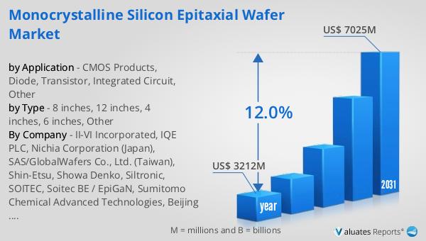
Global Monocrystalline Silicon Epitaxial Wafer Market Outlook:
The global market for Monocrystalline Silicon Epitaxial Wafer was valued at $3,212 million in 2024 and is anticipated to expand to a revised size of $7,025 million by 2031, reflecting a compound annual growth rate (CAGR) of 12.0% over the forecast period. Despite being the largest region, Asia Pacific experienced a decline of 2.0 percent. In contrast, sales in the Americas reached $142.1 billion, marking a 17.0% increase year-on-year. European sales were recorded at $53.8 billion, up 12.6% year-on-year, while sales in Japan amounted to $48.1 billion, reflecting a 10.0% year-on-year increase. However, the Asia-Pacific region, despite its size, saw sales of $336.2 billion, which represented a 2.0% year-on-year decrease. This market outlook highlights the dynamic nature of the global monocrystalline silicon epitaxial wafer market, with varying growth rates across different regions. The robust growth in the Americas, Europe, and Japan underscores the increasing demand for advanced semiconductor technologies in these regions. Meanwhile, the decline in the Asia-Pacific region suggests potential challenges or shifts in market dynamics that may need to be addressed to sustain growth. Overall, the market's projected expansion reflects the ongoing advancements in semiconductor technology and the growing demand for high-performance electronic components worldwide.
| Report Metric | Details |
| Report Name | Monocrystalline Silicon Epitaxial Wafer Market |
| Accounted market size in year | US$ 3212 million |
| Forecasted market size in 2031 | US$ 7025 million |
| CAGR | 12.0% |
| Base Year | year |
| Forecasted years | 2025 - 2031 |
| by Type |
|
| by Application |
|
| Production by Region |
|
| Consumption by Region |
|
| By Company | II-VI Incorporated, IQE PLC, Nichia Corporation (Japan), SAS/GlobalWafers Co., Ltd. (Taiwan), Shin-Etsu, Showa Denko, Siltronic, SOITEC, Soitec BE / EpiGaN, Sumitomo Chemical Advanced Technologies, Beijing Eswell Technology Group Co., Ltd., Hebei Puxing Electronic Technology Co., Ltd., Nanjing Guosheng Electronics Co., Ltd., Shanghai Xinao Technology Co., Ltd., Zhejiang Jinruihong Technology Co., Ltd. |
| Forecast units | USD million in value |
| Report coverage | Revenue and volume forecast, company share, competitive landscape, growth factors and trends |