What is Global Wafer Bonding Equipment Market?
The Global Wafer Bonding Equipment Market refers to the industry focused on the production and sale of machinery used to bond wafers. Wafers are thin slices of semiconductor material, such as silicon, used in electronics for the fabrication of integrated circuits and other microdevices. Wafer bonding is a critical process in semiconductor manufacturing, where two or more wafers are joined together to create a single, unified structure. This process is essential for creating complex electronic components and systems, including microelectromechanical systems (MEMS), advanced packaging solutions, and various types of sensors. The market for wafer bonding equipment is driven by the increasing demand for miniaturized electronic devices, advancements in semiconductor technology, and the growing need for efficient and reliable bonding solutions. As technology continues to evolve, the demand for high-quality wafer bonding equipment is expected to rise, making it a vital component of the semiconductor manufacturing industry. The market encompasses a range of equipment types, including fully automatic and semi-automatic systems, each designed to meet specific manufacturing needs and production scales.
Fully Automatic, Semi Automatic in the Global Wafer Bonding Equipment Market:
In the Global Wafer Bonding Equipment Market, equipment is generally categorized into two main types: fully automatic and semi-automatic systems. Fully automatic wafer bonding equipment is designed to perform the bonding process with minimal human intervention. These systems are equipped with advanced robotics and automation technologies that allow for precise control over the bonding process, ensuring high accuracy and repeatability. Fully automatic systems are ideal for high-volume production environments where efficiency and consistency are paramount. They are often used in large-scale semiconductor manufacturing facilities where the demand for rapid production and high throughput is critical. These systems can handle a wide range of wafer sizes and materials, making them versatile and adaptable to various manufacturing requirements. On the other hand, semi-automatic wafer bonding equipment requires some level of human involvement in the bonding process. While these systems still incorporate automation technologies, they allow operators to manually control certain aspects of the process, providing greater flexibility and control. Semi-automatic systems are often used in research and development settings or smaller production environments where customization and adaptability are more important than sheer volume. These systems are typically more cost-effective than fully automatic systems, making them an attractive option for smaller companies or those with limited budgets. Both fully automatic and semi-automatic wafer bonding equipment play crucial roles in the semiconductor manufacturing industry, each offering unique advantages depending on the specific needs and goals of the manufacturer. As the demand for advanced electronic devices continues to grow, the need for efficient and reliable wafer bonding solutions will remain a key driver of the market.
MEMS, Advanced Packaging, CIS, Others in the Global Wafer Bonding Equipment Market:
The Global Wafer Bonding Equipment Market finds its applications in various areas, including MEMS, advanced packaging, CIS, and others. In the realm of MEMS (Microelectromechanical Systems), wafer bonding equipment is used to create devices that integrate mechanical and electrical components on a single chip. MEMS devices are used in a wide range of applications, from automotive sensors to medical devices, and require precise and reliable bonding techniques to ensure their functionality and performance. Advanced packaging is another critical area where wafer bonding equipment is utilized. This involves the integration of multiple semiconductor devices into a single package, enhancing performance and reducing size. Wafer bonding plays a crucial role in advanced packaging by enabling the stacking and interconnection of multiple wafers, leading to more compact and efficient electronic systems. In the field of CIS (CMOS Image Sensors), wafer bonding equipment is used to create high-performance imaging devices. CIS technology is widely used in digital cameras, smartphones, and other imaging applications, where high-quality image capture is essential. Wafer bonding allows for the integration of different materials and technologies, resulting in improved image quality and sensor performance. Beyond these specific areas, wafer bonding equipment is also used in various other applications, including the production of power devices, RF components, and optoelectronic devices. The versatility and adaptability of wafer bonding equipment make it an essential tool in the semiconductor manufacturing industry, supporting the development of a wide range of electronic devices and systems. As technology continues to advance, the demand for high-quality wafer bonding solutions will remain strong, driving innovation and growth in the market.
Global Wafer Bonding Equipment Market Outlook:
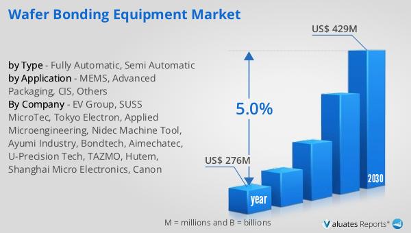
The global market for Wafer Bonding Equipment was valued at approximately $321 million in 2024, with projections indicating a growth to around $449 million by 2031. This growth represents a compound annual growth rate (CAGR) of 5.0% over the forecast period. This steady increase in market size reflects the growing demand for advanced semiconductor manufacturing solutions, driven by the rapid evolution of technology and the increasing need for miniaturized electronic devices. As industries such as consumer electronics, automotive, and telecommunications continue to expand, the demand for efficient and reliable wafer bonding equipment is expected to rise. The market's growth is also supported by ongoing advancements in semiconductor technology, which require more sophisticated and precise bonding solutions. As a result, manufacturers are investing in the development of new and improved wafer bonding equipment to meet the evolving needs of the industry. This growth trajectory highlights the importance of wafer bonding equipment in the semiconductor manufacturing process and underscores the critical role it plays in enabling the production of advanced electronic devices. As the market continues to expand, companies operating in this space will need to focus on innovation and quality to maintain their competitive edge and capitalize on the growing opportunities in the industry.
| Report Metric | Details |
| Report Name | Wafer Bonding Equipment Market |
| Accounted market size in year | US$ 321 million |
| Forecasted market size in 2031 | US$ 449 million |
| CAGR | 5.0% |
| Base Year | year |
| Forecasted years | 2025 - 2031 |
| by Type |
|
| by Application |
|
| Production by Region |
|
| Consumption by Region |
|
| By Company | EV Group, SUSS MicroTec, Tokyo Electron, Applied Microengineering, Nidec Machine Tool, Ayumi Industry, Bondtech, Aimechatec, U-Precision Tech, TAZMO, Hutem, Shanghai Micro Electronics, Canon |
| Forecast units | USD million in value |
| Report coverage | Revenue and volume forecast, company share, competitive landscape, growth factors and trends |


