What is Global High Voltage (HV) Wafer Foundry Market?
The Global High Voltage (HV) Wafer Foundry Market is a specialized segment within the semiconductor industry that focuses on the production of high voltage wafers. These wafers are essential components in the manufacturing of various electronic devices that require high voltage operations. The foundry market is characterized by its ability to produce wafers that can handle high voltage levels, which are crucial for applications in power electronics, automotive, telecommunications, and industrial sectors. The demand for high voltage wafers is driven by the increasing need for efficient power management solutions and the growing adoption of electric vehicles and renewable energy systems. Foundries in this market are equipped with advanced technologies and processes to produce high-quality wafers that meet the stringent requirements of high voltage applications. The market is also influenced by factors such as technological advancements, increasing investments in research and development, and the rising demand for energy-efficient electronic devices. As a result, the Global High Voltage Wafer Foundry Market is expected to witness significant growth in the coming years, driven by the increasing demand for high voltage applications across various industries.
in the Global High Voltage (HV) Wafer Foundry Market:
In the Global High Voltage (HV) Wafer Foundry Market, various types of wafers are utilized by customers based on their specific needs and applications. These types include silicon wafers, silicon carbide (SiC) wafers, and gallium nitride (GaN) wafers, each offering unique properties and advantages. Silicon wafers are the most commonly used type in the semiconductor industry due to their cost-effectiveness and well-established manufacturing processes. They are widely used in applications that require moderate voltage levels and are suitable for a range of electronic devices. However, as the demand for higher efficiency and performance increases, alternative materials like silicon carbide and gallium nitride are gaining popularity. Silicon carbide wafers are known for their ability to operate at higher temperatures and voltages, making them ideal for high-power applications such as electric vehicles, industrial motors, and power grids. They offer superior thermal conductivity and energy efficiency, which are critical for reducing energy losses in high voltage applications. Gallium nitride wafers, on the other hand, are recognized for their high electron mobility and efficiency in converting electrical energy. They are increasingly used in applications that require high frequency and high power, such as radio frequency amplifiers, power converters, and wireless charging systems. The choice of wafer type depends on factors such as the required voltage level, operating environment, and cost considerations. Customers in the Global High Voltage Wafer Foundry Market carefully evaluate these factors to select the most suitable wafer type for their specific applications. Additionally, advancements in wafer manufacturing technologies have led to the development of new materials and processes that enhance the performance and reliability of high voltage wafers. For instance, the introduction of advanced epitaxial growth techniques and the use of innovative doping methods have improved the electrical properties of wafers, enabling them to handle higher voltages and currents. Moreover, the increasing focus on sustainability and energy efficiency has driven the demand for wafers that can support the development of eco-friendly technologies. As a result, foundries are investing in research and development to create wafers that meet the evolving needs of customers in the high voltage market. The collaboration between wafer foundries and end-users is also crucial in driving innovation and ensuring that the wafers produced meet the specific requirements of different applications. By understanding the diverse needs of customers and leveraging advanced technologies, the Global High Voltage Wafer Foundry Market continues to evolve and expand, offering a wide range of wafer types to cater to the growing demand for high voltage applications.
in the Global High Voltage (HV) Wafer Foundry Market:
The Global High Voltage (HV) Wafer Foundry Market serves a wide range of applications across various industries, each requiring high voltage wafers for different purposes. One of the primary applications is in the power electronics sector, where high voltage wafers are used in devices such as power transistors, diodes, and thyristors. These components are essential for controlling and converting electrical power in systems like power supplies, inverters, and motor drives. The ability of high voltage wafers to handle large amounts of power efficiently makes them ideal for these applications, where energy efficiency and reliability are critical. Another significant application of high voltage wafers is in the automotive industry, particularly in electric vehicles (EVs) and hybrid electric vehicles (HEVs). As the demand for cleaner and more efficient transportation solutions grows, the need for high voltage components in EVs and HEVs has increased. High voltage wafers are used in power modules and converters that manage the flow of electricity between the battery and the electric motor, ensuring optimal performance and efficiency. In the telecommunications industry, high voltage wafers are used in the production of radio frequency (RF) amplifiers and other communication devices that require high power and frequency capabilities. These wafers enable the development of advanced communication systems that support high-speed data transmission and improved connectivity. Additionally, the industrial sector relies on high voltage wafers for applications such as industrial automation, robotics, and renewable energy systems. In industrial automation, high voltage components are used in motor drives and control systems that require precise power management and high efficiency. In renewable energy systems, high voltage wafers are used in power converters and inverters that facilitate the integration of solar and wind energy into the power grid. The ability of high voltage wafers to operate at high temperatures and voltages makes them suitable for these demanding applications, where performance and reliability are paramount. Furthermore, the medical industry also utilizes high voltage wafers in medical imaging equipment and diagnostic devices that require high power and precision. The use of high voltage wafers in these applications ensures accurate and reliable performance, which is crucial for patient safety and effective diagnosis. Overall, the Global High Voltage Wafer Foundry Market plays a vital role in supporting the development of advanced technologies across various industries, enabling the creation of innovative solutions that meet the growing demand for high voltage applications.
Global High Voltage (HV) Wafer Foundry Market Outlook:
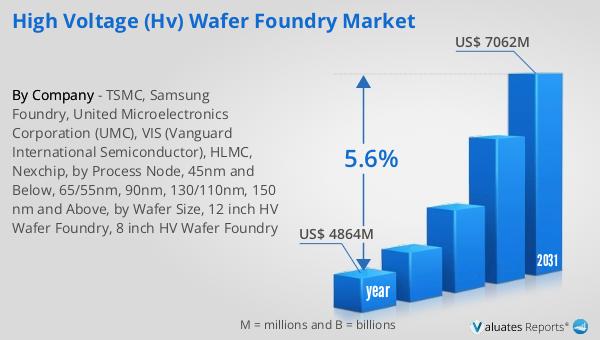
The global market for High Voltage HV Wafer Foundry was valued at approximately $4,864 million in 2024. Over the years, this market is anticipated to grow significantly, reaching an estimated size of $7,062 million by 2031. This growth trajectory represents a compound annual growth rate (CAGR) of 5.6% during the forecast period. The steady increase in market size reflects the rising demand for high voltage wafers across various industries, driven by the need for efficient power management solutions and the growing adoption of electric vehicles and renewable energy systems. The market's expansion is also supported by technological advancements and increasing investments in research and development, which have led to the development of high-performance wafers that meet the stringent requirements of high voltage applications. As industries continue to seek innovative solutions to enhance energy efficiency and reduce environmental impact, the demand for high voltage wafers is expected to rise, contributing to the market's growth. The Global High Voltage Wafer Foundry Market is poised for significant expansion, offering opportunities for manufacturers and suppliers to capitalize on the increasing demand for high voltage applications.
| Report Metric | Details |
| Report Name | High Voltage (HV) Wafer Foundry Market |
| Accounted market size in year | US$ 4864 million |
| Forecasted market size in 2031 | US$ 7062 million |
| CAGR | 5.6% |
| Base Year | year |
| Forecasted years | 2025 - 2031 |
| Production by Region |
|
| Consumption by Region |
|
| By Company | TSMC, Samsung Foundry, United Microelectronics Corporation (UMC), VIS (Vanguard International Semiconductor), HLMC, Nexchip, by Process Node, 45nm and Below, 65/55nm, 90nm, 130/110nm, 150 nm and Above, by Wafer Size, 12 inch HV Wafer Foundry, 8 inch HV Wafer Foundry |
| Forecast units | USD million in value |
| Report coverage | Revenue and volume forecast, company share, competitive landscape, growth factors and trends |


