What is Global BCD Process Wafer Foundry Market?
The Global BCD Process Wafer Foundry Market is a specialized segment within the semiconductor industry that focuses on the production of wafers using BCD (Bipolar-CMOS-DMOS) technology. This technology integrates three different types of transistors—bipolar, CMOS, and DMOS—onto a single chip, allowing for the creation of highly efficient and versatile electronic components. BCD technology is particularly valued for its ability to handle high voltages and currents, making it ideal for power management applications. Foundries that specialize in BCD process wafers provide essential services to a wide range of industries, including automotive, consumer electronics, and industrial sectors. These foundries offer the infrastructure and expertise needed to produce complex semiconductor devices that meet the specific requirements of their clients. As demand for more efficient and compact electronic devices continues to grow, the BCD Process Wafer Foundry Market plays a crucial role in enabling technological advancements and innovation. The market is characterized by continuous research and development efforts aimed at improving the performance and cost-effectiveness of BCD technology, ensuring its relevance in an ever-evolving technological landscape.
in the Global BCD Process Wafer Foundry Market:
The Global BCD Process Wafer Foundry Market caters to a diverse array of customer needs by offering various types of BCD process technologies. Each type is designed to meet specific performance criteria and application requirements, making them suitable for different industries and use cases. One of the primary types is the standard BCD process, which is widely used for general-purpose applications. This type offers a balanced combination of bipolar, CMOS, and DMOS transistors, providing a versatile solution for a range of electronic devices. Another type is the high-voltage BCD process, which is specifically designed to handle higher voltage levels. This makes it ideal for applications in power management and automotive electronics, where the ability to manage high voltages is crucial. The high-voltage BCD process ensures that devices can operate efficiently and safely under demanding conditions. Additionally, there is the high-density BCD process, which focuses on maximizing the number of transistors on a single chip. This type is particularly useful for consumer electronics, where space is at a premium and there is a need for compact yet powerful components. The high-density BCD process allows manufacturers to create smaller devices without compromising on performance. Furthermore, the low-power BCD process is tailored for applications that require minimal energy consumption. This type is essential for battery-operated devices, such as smartphones and portable gadgets, where extending battery life is a key concern. By reducing power consumption, the low-power BCD process helps in creating energy-efficient products that align with the growing demand for sustainable technology. Each of these BCD process types is supported by a range of foundry services, including design support, prototyping, and volume production. Foundries work closely with their customers to ensure that the chosen BCD process meets the specific needs of the application, providing customized solutions that enhance the performance and reliability of the final product. As technology continues to evolve, the Global BCD Process Wafer Foundry Market remains committed to developing new and improved process types that address emerging challenges and opportunities in the semiconductor industry.
Smart Phone, Automotive Electronics, Consumer Electronics, Industrial in the Global BCD Process Wafer Foundry Market:
The Global BCD Process Wafer Foundry Market finds extensive usage across various sectors, including smartphones, automotive electronics, consumer electronics, and industrial applications. In the realm of smartphones, BCD technology is instrumental in power management and signal processing. The integration of bipolar, CMOS, and DMOS transistors on a single chip allows for efficient power distribution and management, which is crucial for maintaining battery life and ensuring optimal performance. As smartphones become more advanced, with features such as fast charging and high-resolution displays, the demand for BCD process wafers continues to grow. In automotive electronics, BCD technology plays a vital role in managing the complex electronic systems found in modern vehicles. From engine control units to advanced driver-assistance systems (ADAS), BCD process wafers are used to ensure reliable and efficient operation. The high-voltage capabilities of BCD technology make it particularly suitable for automotive applications, where the ability to handle high power levels is essential. In consumer electronics, BCD process wafers are used in a wide range of devices, from televisions to home appliances. The versatility of BCD technology allows manufacturers to create products that are both powerful and energy-efficient, meeting the demands of today's tech-savvy consumers. The high-density BCD process, in particular, is favored for its ability to pack more functionality into smaller devices, catering to the trend of miniaturization in consumer electronics. In industrial applications, BCD process wafers are used in equipment that requires robust and reliable electronic components. This includes machinery used in manufacturing, automation systems, and energy management solutions. The durability and efficiency of BCD technology make it an ideal choice for industrial environments, where performance and reliability are paramount. As industries continue to embrace digital transformation and automation, the demand for BCD process wafers is expected to rise, further solidifying their importance in the global market.
Global BCD Process Wafer Foundry Market Outlook:
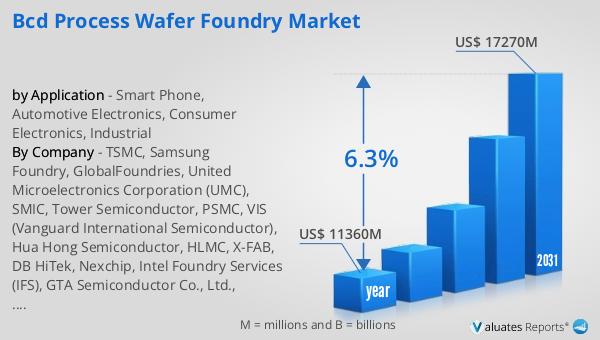
The outlook for the Global BCD Process Wafer Foundry Market is promising, with significant growth anticipated over the coming years. In 2024, the market was valued at approximately $11,360 million, reflecting its substantial role in the semiconductor industry. By 2031, it is projected to reach a revised size of $17,270 million, driven by a compound annual growth rate (CAGR) of 6.3% during the forecast period. This growth is indicative of the increasing demand for BCD process wafers across various sectors, including automotive, consumer electronics, and industrial applications. The market's expansion is fueled by the continuous advancements in technology and the growing need for efficient and compact electronic components. As industries strive to enhance their products' performance and energy efficiency, the reliance on BCD technology is expected to intensify. The market's positive trajectory underscores the importance of BCD process wafers in enabling innovation and meeting the evolving needs of modern technology. With ongoing research and development efforts, the Global BCD Process Wafer Foundry Market is well-positioned to capitalize on emerging opportunities and maintain its relevance in the dynamic semiconductor landscape.
| Report Metric | Details |
| Report Name | BCD Process Wafer Foundry Market |
| Accounted market size in year | US$ 11360 million |
| Forecasted market size in 2031 | US$ 17270 million |
| CAGR | 6.3% |
| Base Year | year |
| Forecasted years | 2025 - 2031 |
| by Application |
|
| Production by Region |
|
| Consumption by Region |
|
| By Company | TSMC, Samsung Foundry, GlobalFoundries, United Microelectronics Corporation (UMC), SMIC, Tower Semiconductor, PSMC, VIS (Vanguard International Semiconductor), Hua Hong Semiconductor, HLMC, X-FAB, DB HiTek, Nexchip, Intel Foundry Services (IFS), GTA Semiconductor Co., Ltd., CanSemi, Polar Semiconductor, LLC, Silterra, SK keyfoundry Inc., by BCD Technology, 12-inch BCD (Bipolar-CMOS-DMOS), 8-inch BCD (Bipolar-CMOS-DMOS), 6-inch BCD (Bipolar-CMOS-DMOS) |
| Forecast units | USD million in value |
| Report coverage | Revenue and volume forecast, company share, competitive landscape, growth factors and trends |


