What is Global AFM for Semiconductor Market?
The Global AFM for Semiconductor Market refers to the worldwide industry focused on the use of Atomic Force Microscopy (AFM) technology within the semiconductor sector. AFM is a type of scanning probe microscopy that provides high-resolution imaging at the nanoscale, making it an invaluable tool for semiconductor manufacturing and research. This market encompasses the development, production, and application of AFM instruments specifically designed to meet the needs of semiconductor companies. These instruments are used to analyze and measure the surface properties of semiconductor materials, ensuring quality control and aiding in the development of new technologies. The market is driven by the increasing demand for miniaturized electronic devices, which require precise and accurate measurement techniques. As semiconductor technology continues to advance, the need for sophisticated tools like AFM grows, making this market a critical component of the broader semiconductor industry. The Global AFM for Semiconductor Market is characterized by ongoing innovation, with companies continually seeking to improve the capabilities and efficiency of AFM instruments to meet the evolving demands of the semiconductor sector.
Small Sample AFM, Large Sample AFM in the Global AFM for Semiconductor Market:
In the Global AFM for Semiconductor Market, there are two primary types of Atomic Force Microscopes: Small Sample AFM and Large Sample AFM. Small Sample AFM is designed for analyzing smaller semiconductor samples, typically used in research and development settings. These instruments are compact and offer high precision, making them ideal for detailed surface analysis at the nanoscale. They are often used in laboratories where space is limited, and the focus is on developing new semiconductor materials and technologies. Small Sample AFMs are equipped with advanced features such as high-resolution imaging and the ability to measure various surface properties, including roughness, hardness, and electrical conductivity. These capabilities are crucial for researchers who need to understand the intricate details of semiconductor materials to innovate and improve their performance. On the other hand, Large Sample AFM is tailored for handling bigger semiconductor samples, which are often encountered in industrial and manufacturing environments. These instruments are designed to accommodate larger wafers and substrates, making them suitable for quality control and inspection processes in semiconductor fabrication plants. Large Sample AFMs provide a broader range of motion and can scan larger areas, which is essential for ensuring the uniformity and quality of semiconductor products. They are equipped with robust scanning capabilities and can perform comprehensive surface analyses, including defect detection and thickness measurement. This makes them indispensable tools for manufacturers who need to maintain high standards of quality and reliability in their semiconductor products. Both Small Sample AFM and Large Sample AFM play crucial roles in the semiconductor industry, each catering to different needs and applications. While Small Sample AFMs are more suited for research and development, Large Sample AFMs are essential for production and quality assurance. The choice between the two depends on the specific requirements of the semiconductor company, including the size of the samples they work with and the nature of their operations. As the semiconductor industry continues to evolve, the demand for both types of AFM is expected to grow, driven by the need for more precise and efficient measurement tools. Companies in the Global AFM for Semiconductor Market are continually innovating to enhance the capabilities of both Small and Large Sample AFMs, ensuring they meet the ever-changing demands of the industry.
In-Line Metrology, Surface Topography, Surface Impurity Analysis, Others in the Global AFM for Semiconductor Market:
The Global AFM for Semiconductor Market finds extensive usage in various areas, including In-Line Metrology, Surface Topography, Surface Impurity Analysis, and other applications. In-Line Metrology is a critical application of AFM technology in the semiconductor industry. It involves the real-time measurement and analysis of semiconductor wafers during the manufacturing process. AFM instruments are used to monitor the dimensions and surface properties of wafers, ensuring they meet the required specifications. This application is essential for maintaining the quality and consistency of semiconductor products, as it allows manufacturers to detect and correct any deviations in real-time. By integrating AFM technology into the production line, semiconductor companies can achieve higher yields and reduce the risk of defects, ultimately improving the efficiency and profitability of their operations. Surface Topography is another important application of AFM in the semiconductor market. It involves the detailed analysis of the surface features of semiconductor materials, including their roughness, texture, and morphology. AFM instruments provide high-resolution imaging capabilities, allowing researchers and manufacturers to visualize and measure the nanoscale features of semiconductor surfaces. This information is crucial for understanding the performance and reliability of semiconductor devices, as surface characteristics can significantly impact their electrical and mechanical properties. By using AFM for surface topography analysis, semiconductor companies can optimize their materials and processes, leading to the development of more advanced and efficient devices. Surface Impurity Analysis is a key application of AFM technology in the semiconductor industry. It involves the detection and characterization of impurities and contaminants on the surface of semiconductor materials. AFM instruments are capable of identifying and quantifying various types of impurities, including particles, residues, and chemical contaminants. This application is vital for ensuring the purity and quality of semiconductor products, as impurities can adversely affect their performance and reliability. By using AFM for surface impurity analysis, semiconductor companies can implement effective contamination control measures, reducing the risk of defects and improving the overall quality of their products. In addition to these applications, AFM technology is used in various other areas within the semiconductor industry. For example, it is employed in the development and testing of new semiconductor materials, where it provides valuable insights into their properties and performance. AFM is also used in failure analysis, helping companies identify the root causes of defects and implement corrective actions. Furthermore, AFM technology is used in research and development, where it supports the innovation of new semiconductor technologies and devices. Overall, the Global AFM for Semiconductor Market plays a crucial role in advancing the semiconductor industry, providing the tools and capabilities needed to meet the growing demands for high-performance and reliable semiconductor products.
Global AFM for Semiconductor Market Outlook:
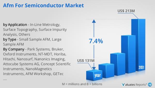
In 2024, the global market for AFM in the semiconductor sector was valued at approximately US$ 131 million. This market is anticipated to expand significantly, reaching an estimated size of US$ 213 million by 2031. This growth trajectory represents a compound annual growth rate (CAGR) of 7.4% over the forecast period. Such a robust growth rate underscores the increasing importance and adoption of AFM technology in the semiconductor industry. The market's expansion is driven by the continuous advancements in semiconductor technology and the rising demand for precise and accurate measurement tools. As semiconductor devices become more complex and miniaturized, the need for high-resolution imaging and analysis provided by AFM instruments becomes even more critical. The market is characterized by the presence of several key players, with the top three international companies holding a cumulative market share of over 35%. This concentration of market share among leading companies highlights the competitive nature of the industry and the importance of innovation and technological advancements in maintaining a strong market position. These companies are at the forefront of developing cutting-edge AFM instruments that cater to the evolving needs of the semiconductor sector. Their focus on research and development, coupled with strategic partnerships and collaborations, enables them to offer advanced solutions that enhance the capabilities and efficiency of semiconductor manufacturing processes. Overall, the Global AFM for Semiconductor Market is poised for significant growth, driven by the increasing demand for high-performance semiconductor devices and the need for advanced measurement and analysis tools. As the market continues to evolve, companies will need to focus on innovation and technological advancements to maintain their competitive edge and capitalize on the opportunities presented by the growing semiconductor industry.
| Report Metric | Details |
| Report Name | AFM for Semiconductor Market |
| Accounted market size in year | US$ 131 million |
| Forecasted market size in 2031 | US$ 213 million |
| CAGR | 7.4% |
| Base Year | year |
| Forecasted years | 2025 - 2031 |
| by Type |
|
| by Application |
|
| Production by Region |
|
| Consumption by Region |
|
| By Company | Park Systems, Bruker, Oxford Instruments, NT-MDT, Horiba, Hitachi, Nanosurf, Nanonics Imaging, Attocube Systems AG, Concept Scientific Instruments, NanoMagnetics Instruments, AFM Workshop, GETec Microscopy, A.P.E Research, RHK Technology |
| Forecast units | USD million in value |
| Report coverage | Revenue and volume forecast, company share, competitive landscape, growth factors and trends |


