Saturday, August 16, 2025

Global Wafer Shipment Containers Market Research Report 2025

What is Global Wafer Shipment Containers Market?

The Global Wafer Shipment Containers Market is a specialized segment within the semiconductor industry, focusing on the transportation and storage of semiconductor wafers. These containers are crucial for maintaining the integrity and quality of wafers during transit from manufacturing facilities to various processing plants. Wafers, being extremely delicate and sensitive to contamination, require robust and reliable packaging solutions. The market for wafer shipment containers is driven by the increasing demand for semiconductors across various industries, including electronics, automotive, and telecommunications. As technology advances, the need for more sophisticated and high-capacity wafers grows, further propelling the demand for efficient shipment containers. These containers are designed to protect wafers from physical damage, contamination, and environmental factors such as humidity and temperature fluctuations. The market is characterized by continuous innovation, with manufacturers striving to develop containers that offer enhanced protection and efficiency. The growth of the semiconductor industry, coupled with the increasing complexity of wafer designs, is expected to drive the demand for wafer shipment containers in the coming years. The market is also influenced by regional manufacturing trends, with key players focusing on expanding their presence in high-demand areas.

Wafer Shipment Containers Market

FOUP, FOSB in the Global Wafer Shipment Containers Market:

Front Opening Unified Pods (FOUP) and Front Opening Shipping Boxes (FOSB) are integral components of the Global Wafer Shipment Containers Market, each serving distinct roles in the handling and transportation of semiconductor wafers. FOUPs are specialized containers designed to hold and transport wafers within semiconductor fabrication facilities. They are engineered to provide a controlled environment that minimizes contamination and mechanical damage to the wafers. FOUPs are typically used in cleanroom environments and are compatible with automated material handling systems, which are essential in modern semiconductor manufacturing processes. These containers are made from high-grade materials that ensure durability and protection against electrostatic discharge, which can damage sensitive semiconductor components. The design of FOUPs allows for easy integration with robotic systems, facilitating efficient wafer handling and reducing the risk of human error. On the other hand, FOSBs are primarily used for the transportation of wafers between different facilities or from suppliers to manufacturers. They are designed to provide robust protection against physical shocks and environmental factors during transit. FOSBs are typically larger than FOUPs and are constructed to withstand the rigors of shipping and handling. They are equipped with features such as shock absorbers and secure locking mechanisms to ensure the safe transport of wafers over long distances. The use of FOSBs is critical in maintaining the quality and integrity of wafers as they move through the supply chain. Both FOUPs and FOSBs play a vital role in the semiconductor manufacturing process, ensuring that wafers are protected from contamination and damage at every stage of production and transportation. The demand for these containers is driven by the increasing complexity of semiconductor devices and the need for higher levels of precision and reliability in wafer handling. As the semiconductor industry continues to evolve, the design and functionality of FOUPs and FOSBs are expected to advance, offering even greater levels of protection and efficiency. Manufacturers are investing in research and development to create containers that meet the stringent requirements of modern semiconductor manufacturing, including the ability to handle larger wafer sizes and more complex device architectures. The market for FOUPs and FOSBs is also influenced by regional manufacturing trends, with key players focusing on expanding their presence in high-demand areas. As the global demand for semiconductors continues to rise, the importance of reliable and efficient wafer shipment containers like FOUPs and FOSBs cannot be overstated. These containers are essential for ensuring the smooth operation of semiconductor manufacturing processes and the delivery of high-quality products to end-users.

300 mm Wafer, 200 mm Wafer in the Global Wafer Shipment Containers Market:

The Global Wafer Shipment Containers Market plays a crucial role in the handling and transportation of 300 mm and 200 mm wafers, which are widely used in the semiconductor industry. The 300 mm wafer, being larger in size, offers significant advantages in terms of cost efficiency and production capacity. However, its larger size also presents challenges in terms of handling and transportation. Wafer shipment containers designed for 300 mm wafers are engineered to provide maximum protection against physical damage and contamination. These containers are equipped with advanced features such as shock absorbers and secure locking mechanisms to ensure the safe transport of wafers over long distances. The use of 300 mm wafers is prevalent in the production of high-performance semiconductor devices, and the demand for these wafers is driven by the increasing need for advanced electronic products. The Global Wafer Shipment Containers Market is expected to witness significant growth as the demand for 300 mm wafers continues to rise. On the other hand, 200 mm wafers are still widely used in the production of various semiconductor devices, particularly in applications where cost efficiency is a primary concern. The handling and transportation of 200 mm wafers require specialized containers that offer robust protection against contamination and mechanical damage. These containers are designed to accommodate the smaller size of 200 mm wafers while providing the same level of protection and efficiency as those used for larger wafers. The demand for 200 mm wafers is driven by the production of a wide range of electronic devices, including consumer electronics, automotive components, and industrial equipment. The Global Wafer Shipment Containers Market is expected to continue to grow as the demand for 200 mm wafers remains strong. The market for wafer shipment containers is characterized by continuous innovation, with manufacturers striving to develop containers that offer enhanced protection and efficiency for both 300 mm and 200 mm wafers. The growth of the semiconductor industry, coupled with the increasing complexity of wafer designs, is expected to drive the demand for wafer shipment containers in the coming years. The market is also influenced by regional manufacturing trends, with key players focusing on expanding their presence in high-demand areas. As the global demand for semiconductors continues to rise, the importance of reliable and efficient wafer shipment containers cannot be overstated. These containers are essential for ensuring the smooth operation of semiconductor manufacturing processes and the delivery of high-quality products to end-users.

Global Wafer Shipment Containers Market Outlook:

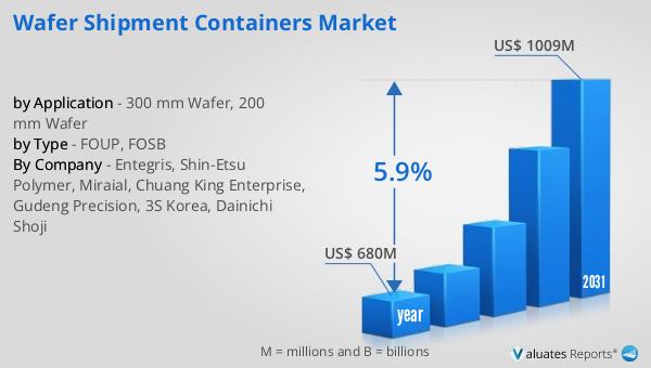
In 2024, the worldwide market for Wafer Shipment Containers was estimated to be worth approximately $680 million. By 2031, this market is anticipated to expand to a revised valuation of $1009 million, reflecting a compound annual growth rate (CAGR) of 5.9% throughout the forecast period. Taiwan emerges as the leading consumer region for wafer cassettes, holding a consumption market share of nearly 19.75% as of 2022. This indicates Taiwan's significant role in the global semiconductor supply chain, driven by its robust manufacturing capabilities and technological advancements. Furthermore, the market is highly consolidated, with the top five companies globally commanding a substantial 96.32% of the total market share. This concentration underscores the dominance of a few key players in the industry, who are likely leveraging their technological expertise, extensive distribution networks, and strategic partnerships to maintain their competitive edge. The growth trajectory of the Wafer Shipment Containers Market is indicative of the increasing demand for semiconductors across various sectors, including electronics, automotive, and telecommunications. As the semiconductor industry continues to evolve, the need for efficient and reliable wafer shipment solutions will remain critical, driving further innovation and development in this market segment.


Report Metric Details
Report Name Wafer Shipment Containers Market
Accounted market size in year US$ 680 million
Forecasted market size in 2031 US$ 1009 million
CAGR 5.9%
Base Year year
Forecasted years 2025 - 2031
by Type
  • FOUP
  • FOSB
by Application
  • 300 mm Wafer
  • 200 mm Wafer
Production by Region
  • North America
  • Europe
  • China
  • Japan
  • South Korea
  • Taiwan
Consumption by Region
  • North America (United States, Canada)
  • Europe (Germany, France, UK, Italy, Russia)
  • Asia-Pacific (China, Japan, South Korea, Taiwan)
  • Southeast Asia (India)
  • Latin America (Mexico, Brazil)
By Company Entegris, Shin-Etsu Polymer, Miraial, Chuang King Enterprise, Gudeng Precision, 3S Korea, Dainichi Shoji
Forecast units USD million in value
Report coverage Revenue and volume forecast, company share, competitive landscape, growth factors and trends

Global Wafer In-Process Containers Market Research Report 2025

What is Global Wafer In-Process Containers Market?

The Global Wafer In-Process Containers Market is a specialized segment within the semiconductor industry that focuses on the storage and transportation of semiconductor wafers during the manufacturing process. These containers are crucial for maintaining the integrity and quality of wafers, which are thin slices of semiconductor material used in the fabrication of integrated circuits and other microdevices. The market for these containers is driven by the increasing demand for semiconductors across various industries, including electronics, automotive, and telecommunications. As technology advances, the need for more sophisticated and reliable wafer handling solutions grows, leading to innovations in container design and materials. The market is characterized by a range of products designed to accommodate different wafer sizes and types, ensuring that they are protected from contamination and physical damage during processing. This market is essential for the efficient and effective production of semiconductors, which are the building blocks of modern electronic devices. As the semiconductor industry continues to expand, the demand for high-quality wafer in-process containers is expected to rise, making this a dynamic and evolving market.

Wafer In-Process Containers Market

PC Resin Materials, PBT Resin Materials, Others in the Global Wafer In-Process Containers Market:

In the Global Wafer In-Process Containers Market, materials such as PC Resin, PBT Resin, and others play a significant role in the manufacturing of containers that ensure the safe handling and transportation of semiconductor wafers. PC Resin, or Polycarbonate Resin, is known for its excellent impact resistance and optical clarity, making it a popular choice for wafer containers. Its durability and ability to withstand high temperatures make it ideal for environments where wafers are processed. PC Resin containers are often used in applications where visibility of the wafer is important, allowing for easy inspection without opening the container. On the other hand, PBT Resin, or Polybutylene Terephthalate Resin, is valued for its high strength and resistance to chemicals and moisture. This makes PBT Resin containers suitable for environments where wafers are exposed to harsh chemicals or require a high degree of cleanliness. PBT Resin's dimensional stability ensures that the containers maintain their shape and integrity under various conditions, providing reliable protection for the wafers. Other materials used in wafer in-process containers include various polymers and composites that offer specific properties tailored to different stages of the semiconductor manufacturing process. These materials are selected based on their ability to provide the necessary protection and support for wafers, ensuring that they remain free from contamination and damage. The choice of material is crucial, as it impacts the overall performance and reliability of the container. Manufacturers in this market continuously explore new materials and technologies to enhance the functionality and efficiency of wafer in-process containers. This includes developing materials that offer improved thermal stability, chemical resistance, and mechanical strength. As the semiconductor industry evolves, the demand for advanced materials in wafer in-process containers is expected to grow, driving innovation and development in this sector. The use of PC Resin, PBT Resin, and other materials in wafer in-process containers highlights the importance of material selection in ensuring the safe and efficient handling of semiconductor wafers. Each material offers unique benefits that cater to specific requirements in the semiconductor manufacturing process, making them integral to the success of the Global Wafer In-Process Containers Market.

300 mm Wafer, 200 mm Wafer, Others in the Global Wafer In-Process Containers Market:

The Global Wafer In-Process Containers Market finds its application in various wafer sizes, including 300 mm wafers, 200 mm wafers, and others. The 300 mm wafer is the largest standard size used in the semiconductor industry, offering significant advantages in terms of cost efficiency and production volume. Containers designed for 300 mm wafers are engineered to accommodate the larger size while providing robust protection against contamination and physical damage. These containers are essential for maintaining the quality and integrity of the wafers throughout the manufacturing process, ensuring that they meet the stringent standards required for high-performance semiconductor devices. The use of 300 mm wafers is prevalent in advanced semiconductor manufacturing facilities, where the focus is on maximizing output and reducing costs. In contrast, 200 mm wafers are smaller and are often used in the production of less complex semiconductor devices. Containers for 200 mm wafers are designed to offer the same level of protection and reliability as those for larger wafers, ensuring that the wafers remain free from defects and contamination. The demand for 200 mm wafer containers is driven by the continued use of these wafers in various applications, including automotive electronics and consumer devices. Other wafer sizes, such as 150 mm and smaller, also require specialized containers to ensure their safe handling and transportation. These containers are designed to meet the specific needs of different wafer sizes, providing the necessary protection and support to maintain wafer quality. The Global Wafer In-Process Containers Market caters to a diverse range of wafer sizes, reflecting the varied requirements of the semiconductor industry. As technology advances and new applications for semiconductors emerge, the demand for wafer in-process containers across different wafer sizes is expected to grow. This growth is driven by the need for reliable and efficient solutions that ensure the safe handling of wafers, regardless of their size. The market's ability to adapt to the changing needs of the semiconductor industry is a testament to its importance and relevance in the production of modern electronic devices.

Global Wafer In-Process Containers Market Outlook:

The global semiconductor market, valued at approximately $579 billion in 2022, is on a growth trajectory, with projections indicating it could reach around $790 billion by 2029. This anticipated growth represents a compound annual growth rate (CAGR) of 6% over the forecast period. This expansion is driven by the increasing demand for semiconductors across various sectors, including consumer electronics, automotive, telecommunications, and industrial applications. As technology continues to evolve, the need for more advanced and efficient semiconductor solutions is becoming increasingly critical. The rise in demand for smart devices, electric vehicles, and advanced communication technologies is fueling the growth of the semiconductor market. Additionally, the ongoing development of new technologies, such as artificial intelligence, the Internet of Things (IoT), and 5G networks, is further driving the demand for semiconductors. These advancements require more sophisticated and powerful semiconductor components, which in turn boosts the market's growth. The projected growth of the semiconductor market underscores the importance of continued innovation and investment in this sector. As the market expands, the need for reliable and efficient wafer in-process containers will also increase, highlighting the interconnected nature of the semiconductor industry and its supporting markets.


Report Metric Details
Report Name Wafer In-Process Containers Market
Accounted market size in year US$ 579 billion
Forecasted market size in 2029 US$ 790 billion
CAGR 6%
Base Year year
Forecasted years 2025 - 2029
by Type
  • PC Resin Materials
  • PBT Resin Materials
  • Others
by Application
  • 300 mm Wafer
  • 200 mm Wafer
  • Others
Production by Region
  • North America
  • Europe
  • China
  • Japan
  • South Korea
  • Taiwan
Consumption by Region
  • North America (United States, Canada)
  • Europe (Germany, France, UK, Italy, Russia)
  • Asia-Pacific (China, Japan, South Korea, Taiwan)
  • Southeast Asia (India)
  • Latin America (Mexico, Brazil)
By Company Entegris, Shin-Etsu Polymer, Miraial Co.,Ltd., 3S Korea, Chuang King Enterprise, ePAK, Dainichi Shoji K.K., Gudeng Precision, E-SUN
Forecast units USD million in value
Report coverage Revenue and volume forecast, company share, competitive landscape, growth factors and trends

Global Load Port Market Research Report 2025

What is Global Load Port Market?

The Global Load Port Market is a crucial component in the semiconductor manufacturing industry, serving as the interface between wafer handling systems and semiconductor processing equipment. Load ports are essential for the efficient transfer of semiconductor wafers into and out of processing tools, ensuring that the delicate wafers are handled with precision and care. These devices are designed to maintain a clean environment, preventing contamination that could compromise the quality of the semiconductor products. The market for load ports is driven by the increasing demand for semiconductors across various industries, including electronics, automotive, and telecommunications. As technology advances, the need for more sophisticated and efficient load port systems grows, leading to innovations in design and functionality. The global load port market is characterized by a range of products that cater to different needs, from basic manual systems to advanced automated solutions. Manufacturers in this market are focused on developing load ports that offer high reliability, speed, and compatibility with various wafer sizes and types. The market's growth is also influenced by the expansion of semiconductor manufacturing facilities worldwide, as companies strive to meet the rising demand for electronic devices.

Load Port Market

Motor Drive Load Port, Air Drive Load Port in the Global Load Port Market:

Motor Drive Load Ports and Air Drive Load Ports are two significant types of load ports within the Global Load Port Market, each offering distinct advantages and applications. Motor Drive Load Ports are equipped with electric motors that facilitate the movement of wafers into and out of processing equipment. These load ports are known for their precision and ability to handle wafers with minimal human intervention, reducing the risk of contamination and damage. The motor-driven mechanism allows for smooth and controlled wafer transfer, making them ideal for high-volume production environments where speed and accuracy are paramount. Motor Drive Load Ports are often used in advanced semiconductor manufacturing facilities that require high throughput and reliability. On the other hand, Air Drive Load Ports utilize pneumatic systems to move wafers. These load ports are favored for their simplicity and cost-effectiveness, as they rely on compressed air to operate. Air Drive Load Ports are typically used in environments where the cost of operation is a significant consideration, and where the production volume may not justify the investment in more complex motor-driven systems. Despite their simplicity, Air Drive Load Ports are capable of providing reliable wafer handling, making them suitable for a variety of applications. Both types of load ports are designed to integrate seamlessly with other semiconductor manufacturing equipment, ensuring a smooth and efficient production process. The choice between Motor Drive and Air Drive Load Ports often depends on the specific requirements of the manufacturing facility, including factors such as production volume, budget, and the level of automation desired. As the semiconductor industry continues to evolve, manufacturers are constantly innovating to improve the performance and capabilities of both Motor Drive and Air Drive Load Ports, ensuring they meet the ever-changing needs of the market.

EFEM, Sorters in the Global Load Port Market:

The Global Load Port Market plays a vital role in the operation of EFEM (Equipment Front End Module) and Sorters, two critical components in semiconductor manufacturing. EFEMs are automated systems that serve as the interface between the cleanroom environment and the processing equipment, ensuring that wafers are transferred safely and efficiently. Load ports are an integral part of EFEMs, providing the necessary interface for wafer transfer. They ensure that wafers are loaded and unloaded with precision, maintaining the cleanliness and integrity of the wafers throughout the process. The use of load ports in EFEMs is essential for maintaining the high standards of cleanliness required in semiconductor manufacturing, as even the smallest contamination can lead to defects in the final product. Sorters, on the other hand, are used to organize and manage wafers as they move through the manufacturing process. Load ports in sorters facilitate the efficient transfer of wafers between different stages of production, ensuring that they are processed in the correct order and without delay. The integration of load ports in sorters helps to streamline the manufacturing process, reducing the risk of errors and improving overall efficiency. In both EFEMs and sorters, load ports are designed to handle wafers with care, minimizing the risk of damage and ensuring that they are processed to the highest standards. The use of load ports in these applications is critical for maintaining the quality and reliability of semiconductor products, as they ensure that wafers are handled with the utmost precision and care. As the demand for semiconductors continues to grow, the role of load ports in EFEMs and sorters becomes increasingly important, driving innovation and development in the Global Load Port Market.

Global Load Port Market Outlook:

In 2024, the Global Load Port Market was valued at approximately $213 million, with projections indicating a growth to around $328 million by 2031, reflecting a compound annual growth rate (CAGR) of 6.4% over the forecast period. Key players in the EFEM and Sorters market include Brooks Automation, RORZE Corporation, Hirata Corporation, Cymechs Inc, and Sinfonia Technology, among others. In 2021, the top four global players held a significant share of about 69% in terms of revenue. Specifically, for EFEM, major players such as RORZE, Brooks Automation, Hirata, Cymechs, and Siasun Robot Automation dominate the market, with the top five players commanding over 90% of the market share. In the Sorters segment, leading companies like Hirata Corporation, RORZE, JEL Corporation, and Brooks Automation hold more than 50% of the market share. The semiconductor market, a key driver for load ports, was estimated at $526.8 billion in 2023 and is expected to reach $780.7 billion by 2030. Furthermore, the semiconductor manufacturing wafer fabrication market is projected to grow from $251.7 billion in 2023 to $506.5 billion by 2030, with a remarkable CAGR of 40.49% during the forecast period.


Report Metric Details
Report Name Load Port Market
Accounted market size in year US$ 213 million
Forecasted market size in 2031 US$ 328 million
CAGR 6.4%
Base Year year
Forecasted years 2025 - 2031
by Type
  • Motor Drive Load Port
  • Air Drive Load Port
by Application
  • EFEM
  • Sorters
Production by Region
  • North America
  • Europe
  • China
  • Japan
Consumption by Region
  • North America (United States, Canada)
  • Europe (Germany, France, UK, Italy, Russia)
  • Asia-Pacific (China, Japan, South Korea, Taiwan)
  • Southeast Asia (India)
  • Latin America (Mexico, Brazil)
By Company TDK, Hirata Corporation, RORZE Corporation, Sinfonia Technology, Brooks Automation, Kensington Laboratories, Nidec (Genmark Automation), Robots and Design (RND), Rexxam Co Ltd, Mindox Techno, Shanghai Fortrend Technology, Siasun Robot & Automation, HIWIN TECHNOLOGIES, Sanwa Engineering Corporation, Huaxin (Jiaxing) Intelligent Manufacturing
Forecast units USD million in value
Report coverage Revenue and volume forecast, company share, competitive landscape, growth factors and trends

Global IC Packaging Solder Ball Market Research Report 2025

What is Global IC Packaging Solder Ball Market?

The Global IC Packaging Solder Ball Market is a crucial segment within the semiconductor industry, focusing on the tiny spheres of solder used to create electrical connections between integrated circuits (ICs) and printed circuit boards (PCBs). These solder balls are essential in the packaging of ICs, ensuring that the chips can be mounted onto boards with precision and reliability. The market encompasses various types of solder balls, including those made from lead and lead-free materials, catering to different technological and environmental requirements. As the demand for smaller, more efficient electronic devices grows, the need for advanced IC packaging solutions, including high-quality solder balls, becomes increasingly important. This market is driven by innovations in electronics, the push for miniaturization, and the global shift towards environmentally friendly manufacturing processes. The solder balls play a pivotal role in ensuring the performance and longevity of electronic devices, making them indispensable in the production of everything from consumer electronics to industrial machinery. As technology continues to evolve, the Global IC Packaging Solder Ball Market is expected to expand, driven by the ongoing advancements in semiconductor technology and the increasing complexity of electronic devices.

IC Packaging Solder Ball Market

Lead Solder Ball, Lead Free Solder Ball in the Global IC Packaging Solder Ball Market:

Lead solder balls and lead-free solder balls are two primary types of solder balls used in the Global IC Packaging Solder Ball Market, each with distinct characteristics and applications. Lead solder balls, traditionally composed of a tin-lead alloy, have been widely used due to their excellent electrical conductivity, low melting point, and ease of use. These properties make them ideal for applications where reliable electrical connections are paramount, and where the manufacturing process can accommodate the use of lead. However, the use of lead in electronics has raised environmental and health concerns, leading to regulatory measures aimed at reducing or eliminating lead in electronic components. This shift has paved the way for lead-free solder balls, which are typically made from alloys such as tin-silver-copper (SAC). Lead-free solder balls offer a more environmentally friendly alternative, aligning with global initiatives to reduce hazardous substances in electronics. Despite their higher melting points and sometimes more challenging processing requirements, lead-free solder balls are increasingly favored in the industry, particularly in regions with strict environmental regulations. The transition from lead to lead-free solder balls has been driven by both regulatory pressures and the growing consumer demand for greener products. Manufacturers have invested in research and development to improve the performance of lead-free solder balls, ensuring they meet the rigorous demands of modern electronic devices. This includes enhancing their mechanical strength, thermal fatigue resistance, and overall reliability. As a result, lead-free solder balls have become a viable and often preferred option for many applications, from consumer electronics to automotive and industrial systems. The choice between lead and lead-free solder balls ultimately depends on various factors, including regulatory requirements, cost considerations, and specific application needs. In some cases, the superior performance characteristics of lead solder balls may still justify their use, particularly in high-reliability applications where the environmental impact is deemed secondary. However, the trend towards lead-free solutions is clear, driven by both legislative mandates and a broader industry commitment to sustainability. As the Global IC Packaging Solder Ball Market continues to evolve, the balance between lead and lead-free options will likely shift further towards environmentally friendly alternatives, reflecting the industry's ongoing adaptation to changing technological and regulatory landscapes. This transition is not without its challenges, as manufacturers must navigate the complexities of developing and implementing new materials and processes. However, the potential benefits in terms of environmental impact, regulatory compliance, and consumer acceptance make the pursuit of lead-free solutions a compelling and necessary endeavor for the industry.

BGA, CSP & WLCSP, Flip-Chip & Others in the Global IC Packaging Solder Ball Market:

The Global IC Packaging Solder Ball Market finds extensive usage in various packaging technologies, including Ball Grid Array (BGA), Chip Scale Package (CSP) & Wafer Level Chip Scale Package (WLCSP), Flip-Chip, and others. Each of these technologies utilizes solder balls to establish reliable electrical connections between the IC and the substrate, playing a critical role in the performance and reliability of electronic devices. BGA is a popular packaging technology that uses solder balls arranged in a grid pattern on the underside of the IC package. This configuration allows for a higher density of connections compared to traditional pin-based packages, enabling more compact and efficient designs. BGA packages are widely used in applications ranging from consumer electronics to telecommunications and automotive systems, where space and performance are critical considerations. CSP and WLCSP are advanced packaging technologies that further miniaturize the IC package, allowing for even smaller and more efficient designs. These technologies use solder balls to connect the IC directly to the substrate, eliminating the need for a separate package. This results in a thinner, lighter, and more cost-effective solution, ideal for applications where size and weight are critical factors, such as mobile devices and wearable technology. Flip-Chip technology is another important application of solder balls, where the IC is mounted upside down on the substrate, with the solder balls providing the electrical connections. This approach allows for a higher density of connections and improved thermal performance, making it suitable for high-performance applications such as processors and graphics chips. The use of solder balls in these technologies is essential for ensuring the reliability and performance of the final product, as they provide the necessary electrical and mechanical connections between the IC and the substrate. The choice of solder ball material and design can significantly impact the performance and reliability of the package, making it a critical consideration in the design and manufacturing process. As the demand for smaller, more efficient electronic devices continues to grow, the importance of advanced packaging technologies and the role of solder balls in these solutions will only increase. The Global IC Packaging Solder Ball Market is poised to benefit from these trends, as manufacturers seek to develop and implement new materials and processes that meet the evolving needs of the industry. This includes the ongoing transition to lead-free solder balls, as well as the development of new alloys and designs that offer improved performance and reliability. The market is also driven by the increasing complexity of electronic devices, which require more advanced packaging solutions to accommodate the growing number of connections and the need for improved thermal and electrical performance. As a result, the Global IC Packaging Solder Ball Market is expected to continue its growth trajectory, driven by the ongoing advancements in semiconductor technology and the increasing demand for smaller, more efficient electronic devices.

Global IC Packaging Solder Ball Market Outlook:

In 2024, the global market for IC Packaging Solder Balls was valued at approximately $251 million. By 2031, it is anticipated to grow to a revised size of around $388 million, reflecting a compound annual growth rate (CAGR) of 6.5% over the forecast period. This growth trajectory underscores the increasing demand for solder balls in the semiconductor industry, driven by advancements in technology and the rising need for efficient electronic packaging solutions. Key players in this market, such as Senju Metal Accurus and DS HiMetal, hold a significant portion of the market share, collectively accounting for over 73% of the global market. Their dominance highlights the competitive landscape of the industry, where innovation and quality are paramount. The market's expansion is fueled by the ongoing shift towards miniaturization and the development of environmentally friendly manufacturing processes. As electronic devices become more complex and compact, the demand for high-quality solder balls that ensure reliable electrical connections and optimal performance continues to rise. This growth is also supported by the increasing adoption of advanced packaging technologies, such as BGA, CSP, and Flip-Chip, which rely heavily on solder balls for their functionality. The market outlook reflects a dynamic and evolving industry, where the pursuit of innovation and sustainability drives the development of new materials and processes. As the global market for IC Packaging Solder Balls continues to expand, it presents significant opportunities for manufacturers and stakeholders to capitalize on the growing demand for advanced electronic packaging solutions.


Report Metric Details
Report Name IC Packaging Solder Ball Market
Accounted market size in year US$ 251 million
Forecasted market size in 2031 US$ 388 million
CAGR 6.5%
Base Year year
Forecasted years 2025 - 2031
by Type
  • Lead Solder Ball
  • Lead Free Solder Ball
by Application
  • BGA
  • CSP & WLCSP
  • Flip-Chip & Others
Production by Region
  • North America
  • Europe
  • China
  • Japan
  • South Korea
Consumption by Region
  • North America (United States, Canada)
  • Europe (Germany, France, UK, Italy, Russia)
  • Asia-Pacific (China, Japan, South Korea, Taiwan)
  • Southeast Asia (India)
  • Latin America (Mexico, Brazil)
By Company Senju Metal, DS HiMetal, MKE, YCTC, Nippon Micrometal, Accurus, PMTC, Shanghai hiking solder material, Shenmao Technology, Indium Corporation, Jovy Systems
Forecast units USD million in value
Report coverage Revenue and volume forecast, company share, competitive landscape, growth factors and trends

Global 3D Automated Optical Inspection Equipment in PCB Market Research Report 2025

What is Global 3D Automated Optical Inspection Equipment in PCB Market?

Global 3D Automated Optical Inspection (AOI) Equipment in the PCB market refers to advanced technology used to inspect printed circuit boards (PCBs) for defects during the manufacturing process. This equipment utilizes 3D imaging to provide a detailed analysis of the PCB, ensuring that all components are correctly placed and soldered. The technology is crucial in maintaining high-quality standards in PCB production, as it can detect issues such as misalignment, missing components, and soldering defects that might not be visible to the naked eye. By using 3D AOI, manufacturers can reduce the risk of faulty products reaching the market, thereby saving costs associated with recalls and repairs. The global demand for this technology is driven by the increasing complexity of PCBs, which are integral to a wide range of electronic devices. As electronics become more sophisticated, the need for precise and reliable inspection methods like 3D AOI becomes even more critical. This market is characterized by continuous innovation, with companies investing in research and development to enhance the capabilities of AOI systems, making them faster, more accurate, and easier to integrate into existing manufacturing processes.

3D Automated Optical Inspection Equipment in PCB Market

Inline 3D AOI, Offline 3D AOI in the Global 3D Automated Optical Inspection Equipment in PCB Market:

Inline 3D AOI and Offline 3D AOI are two primary types of inspection systems used in the Global 3D Automated Optical Inspection Equipment in the PCB market. Inline 3D AOI systems are integrated directly into the production line, allowing for real-time inspection of PCBs as they are manufactured. This integration enables immediate detection and correction of defects, minimizing downtime and ensuring a smooth production process. Inline systems are particularly beneficial in high-volume manufacturing environments where speed and efficiency are critical. They provide continuous monitoring and can quickly alert operators to any issues, allowing for rapid intervention. On the other hand, Offline 3D AOI systems are used separately from the production line. These systems are typically employed for detailed analysis and quality control, often inspecting samples from a batch rather than every single unit. Offline AOI systems are ideal for low-volume production or for manufacturers who require a more thorough inspection process. They offer flexibility, as they can be used to inspect a wide range of PCB designs without disrupting the main production line. Both Inline and Offline 3D AOI systems utilize advanced imaging technology to create a three-dimensional representation of the PCB, which is then analyzed for defects. The choice between Inline and Offline systems depends on various factors, including production volume, the complexity of the PCBs, and the specific quality control requirements of the manufacturer. Inline systems are generally preferred for large-scale operations where speed is essential, while Offline systems are favored in scenarios where detailed inspection and flexibility are more important. Both types of systems contribute significantly to improving the overall quality and reliability of PCBs, which are crucial components in modern electronic devices. As the demand for more complex and miniaturized electronics continues to grow, the role of 3D AOI systems in ensuring the quality and functionality of PCBs becomes increasingly vital. Manufacturers are continually seeking ways to enhance the capabilities of these systems, incorporating features such as artificial intelligence and machine learning to improve accuracy and efficiency. The ongoing development and adoption of Inline and Offline 3D AOI systems reflect the broader trends in the electronics manufacturing industry, where precision, speed, and reliability are paramount.

Automotive Electronics, Consumer Electronics, Industrials, Others in the Global 3D Automated Optical Inspection Equipment in PCB Market:

The usage of Global 3D Automated Optical Inspection Equipment in the PCB market spans several key areas, including automotive electronics, consumer electronics, industrials, and others. In the automotive electronics sector, 3D AOI systems are essential for ensuring the reliability and safety of electronic components used in vehicles. As cars become increasingly reliant on electronic systems for functions such as navigation, entertainment, and safety features, the need for high-quality PCBs becomes critical. 3D AOI systems help manufacturers detect and correct defects early in the production process, reducing the risk of failures that could lead to costly recalls or safety issues. In the consumer electronics industry, the demand for smaller, more powerful devices drives the need for precise and reliable PCB inspection. 3D AOI systems enable manufacturers to maintain high-quality standards while keeping up with the rapid pace of innovation in this sector. By ensuring that PCBs are free from defects, these systems help prevent issues that could lead to product malfunctions or customer dissatisfaction. In industrial applications, 3D AOI systems are used to inspect PCBs used in a wide range of equipment and machinery. The reliability of these components is crucial, as failures can lead to significant downtime and financial losses. By using 3D AOI systems, manufacturers can ensure that their products meet the stringent quality standards required in industrial settings. Other areas where 3D AOI systems are used include telecommunications, aerospace, and medical devices. In each of these sectors, the quality and reliability of PCBs are of utmost importance, as failures can have serious consequences. 3D AOI systems provide manufacturers with the tools they need to detect and correct defects, ensuring that their products meet the highest standards of quality and performance. As the demand for more complex and reliable electronic devices continues to grow, the role of 3D AOI systems in the PCB market is expected to become even more significant. Manufacturers are continually seeking ways to enhance the capabilities of these systems, incorporating advanced technologies such as artificial intelligence and machine learning to improve accuracy and efficiency. The ongoing development and adoption of 3D AOI systems reflect the broader trends in the electronics manufacturing industry, where precision, speed, and reliability are paramount.

Global 3D Automated Optical Inspection Equipment in PCB Market Outlook:

The global market for 3D Automated Optical Inspection Equipment in PCB was valued at $479 million in 2024, with projections indicating a significant growth trajectory. By 2031, the market is expected to expand to a revised size of $2038 million, reflecting a robust compound annual growth rate (CAGR) of 23.3% over the forecast period. This impressive growth underscores the increasing demand for advanced inspection technologies in the PCB manufacturing sector. As electronic devices become more complex and miniaturized, the need for precise and reliable inspection methods like 3D AOI becomes even more critical. The market's expansion is driven by several factors, including the rising adoption of automation in manufacturing processes, the growing complexity of PCBs, and the increasing demand for high-quality electronic components across various industries. Manufacturers are investing heavily in research and development to enhance the capabilities of 3D AOI systems, making them faster, more accurate, and easier to integrate into existing production lines. This trend is expected to continue as companies seek to maintain a competitive edge in the rapidly evolving electronics market. The projected growth of the 3D AOI market highlights the importance of this technology in ensuring the quality and reliability of PCBs, which are essential components in modern electronic devices.


Report Metric Details
Report Name 3D Automated Optical Inspection Equipment in PCB Market
Accounted market size in year US$ 479 million
Forecasted market size in 2031 US$ 2038 million
CAGR 23.3%
Base Year year
Forecasted years 2025 - 2031
by Type
  • Inline 3D AOI
  • Offline 3D AOI
by Application
  • Automotive Electronics
  • Consumer Electronics
  • Industrials
  • Others
Production by Region
  • North America
  • Europe
  • China
  • Japan
  • South Korea
  • China Taiwan
Consumption by Region
  • North America (United States, Canada)
  • Europe (Germany, France, UK, Italy, Russia)
  • Asia-Pacific (China, Japan, South Korea, Taiwan)
  • Southeast Asia (India)
  • Latin America (Mexico, Brazil)
By Company Koh Young Technology, Mirtec, ViTrox Corporation Berhad, Saki Corporation, Cyberoptics Corporation, Omron Corporation, Viscom, Test Research, Parmi Corp, VI Technology (Mycronic), GÖPEL electronic GmbH, Machine Vision Products (MVP), Mek Marantz Electronics, Pemtron Corp., Nordson YESTECH, JUTZE Intelligence Technology
Forecast units USD million in value
Report coverage Revenue and volume forecast, company share, competitive landscape, growth factors and trends

Global In-line 3D Solder Paste Inspection Equipment Market Research Report 2025

What is Global In-line 3D Solder Paste Inspection Equipment Market?

The Global In-line 3D Solder Paste Inspection Equipment Market is a specialized segment within the electronics manufacturing industry that focuses on the inspection of solder paste applications on printed circuit boards (PCBs).

In-line 3D Solder Paste Inspection Equipment Market

Laser-based 3D Solder Paste Inspection Equipment, PMP-based 3D Solder Paste Inspection Equipment in the Global In-line 3D Solder Paste Inspection Equipment Market:

This market is driven by the increasing demand for high-quality electronic devices, which require precise and reliable soldering processes.

Automotive Electronics, Consumer Electronics, Industrials, Others in the Global In-line 3D Solder Paste Inspection Equipment Market:

In-line 3D solder paste inspection equipment is designed to automatically inspect the solder paste deposits on PCBs during the manufacturing process, ensuring that they meet the required specifications and standards.

Global In-line 3D Solder Paste Inspection Equipment Market Outlook:

This equipment uses advanced imaging and measurement technologies to provide accurate and detailed analysis of the solder paste, helping manufacturers to identify and correct any defects or inconsistencies before the final assembly.


Report Metric Details
Report Name In-line 3D Solder Paste Inspection Equipment Market
Accounted market size in year US$ 309 million
Forecasted market size in 2031 US$ 470 million
CAGR 6.3%
Base Year year
Forecasted years 2025 - 2031
by Type
  • Laser-based 3D Solder Paste Inspection Equipment
  • PMP-based 3D Solder Paste Inspection Equipment
by Application
  • Automotive Electronics
  • Consumer Electronics
  • Industrials
  • Others
Production by Region
  • North America
  • Europe
  • China
  • Japan
  • South Korea
  • China Taiwan
Consumption by Region
  • North America (United States, Canada)
  • Europe (Germany, France, UK, Italy, Russia)
  • Asia-Pacific (China, Japan, South Korea, Taiwan)
  • Southeast Asia (India)
  • Latin America (Mexico, Brazil)
By Company Koh Young, CyberOptics Corporation, Test Research, Inc (TRI), MirTec Ltd, PARMI Corp, Viscom AG, ViTrox, Vi TECHNOLOGY, Mek (Marantz Electronics), Pemtron, SAKI Corporation, Nordson YESTECH, Omron Corporation, Goepel Electronic, Machine Vision Products (MVP), Caltex Scientific, ASC International, Sinic-Tek Vision Technology, Shenzhen JT Automation Equipment, Jet Technology
Forecast units USD million in value
Report coverage Revenue and volume forecast, company share, competitive landscape, growth factors and trends

Global Single-use Bioprocessors Sensors Market Research Report 2025

What is Global Single-use Bioprocessors Sensors Market?

The Global Single-use Bioprocessors Sensors Market is a rapidly evolving sector within the bioprocessing industry, focusing on the development and utilization of disposable sensors designed for single-use applications. These sensors are integral to bioprocessing as they provide critical data on various parameters such as temperature, pH, dissolved oxygen, and pressure, which are essential for maintaining optimal conditions during the production of biopharmaceuticals. The market is driven by the increasing demand for cost-effective and efficient bioprocessing solutions, as single-use sensors eliminate the need for cleaning and sterilization, thereby reducing downtime and operational costs. Additionally, the growing adoption of single-use technologies in the biopharmaceutical industry, coupled with advancements in sensor technology, is expected to propel market growth. The convenience and flexibility offered by these sensors make them an attractive option for both small-scale and large-scale bioprocessing applications. As the industry continues to innovate, the Global Single-use Bioprocessors Sensors Market is poised to play a crucial role in enhancing the efficiency and effectiveness of bioprocessing operations worldwide.

Single-use Bioprocessors Sensors Market

Optical Dissolved Oxygen Sensor, PH Sensor in the Global Single-use Bioprocessors Sensors Market:

Optical Dissolved Oxygen Sensors and pH Sensors are two critical components of the Global Single-use Bioprocessors Sensors Market, each playing a vital role in monitoring and maintaining the optimal conditions required for bioprocessing. Optical Dissolved Oxygen Sensors are designed to measure the concentration of oxygen dissolved in a liquid, which is crucial for aerobic fermentation processes. These sensors utilize optical technology, often based on the principle of fluorescence quenching, to provide accurate and reliable measurements without the need for frequent calibration. The use of optical sensors in single-use bioprocessors offers several advantages, including reduced risk of contamination, ease of integration into disposable systems, and the ability to provide real-time data, which is essential for process control and optimization. On the other hand, pH Sensors are used to measure the acidity or alkalinity of a solution, a critical parameter in bioprocessing as it affects enzyme activity, cell growth, and product stability. Single-use pH Sensors are typically designed with a disposable electrode, eliminating the need for cleaning and maintenance, which can be time-consuming and costly in traditional systems. These sensors are often pre-calibrated and ready to use, providing accurate and consistent measurements that are crucial for maintaining the desired pH levels throughout the bioprocess. The integration of Optical Dissolved Oxygen Sensors and pH Sensors into single-use bioprocessors not only enhances the efficiency and reliability of bioprocessing operations but also supports the industry's shift towards more sustainable and cost-effective solutions. As the demand for biopharmaceuticals continues to rise, the adoption of these advanced sensor technologies is expected to increase, driving further innovation and growth in the Global Single-use Bioprocessors Sensors Market.

Biopharma Industry, Academic Research in the Global Single-use Bioprocessors Sensors Market:

The usage of Global Single-use Bioprocessors Sensors Market in the Biopharma Industry and Academic Research is significant, as these sensors provide critical data that supports the development and production of biopharmaceuticals and the advancement of scientific knowledge. In the Biopharma Industry, single-use sensors are widely used in the production of vaccines, monoclonal antibodies, and other biologics, where maintaining precise control over process parameters is essential for ensuring product quality and safety. The use of single-use sensors allows for greater flexibility and scalability in bioprocessing operations, enabling manufacturers to quickly adapt to changing production demands and reduce the risk of cross-contamination. This is particularly important in the production of personalized medicines, where small batch sizes and rapid turnaround times are required. In Academic Research, single-use bioprocessors sensors are used to study various biological processes and develop new bioprocessing techniques. Researchers benefit from the ease of use and cost-effectiveness of single-use sensors, which allow them to conduct experiments with minimal setup time and reduced risk of contamination. The ability to obtain real-time data on critical process parameters also enables researchers to gain deeper insights into the underlying mechanisms of bioprocessing and develop more efficient and sustainable methods. As the Biopharma Industry and Academic Research continue to evolve, the Global Single-use Bioprocessors Sensors Market is expected to play a crucial role in supporting innovation and driving advancements in bioprocessing technology.

Global Single-use Bioprocessors Sensors Market Outlook:

The global market for Single-use Bioprocessors Sensors was valued at approximately $858 million in 2024, and it is anticipated to grow to a revised size of around $1,132 million by 2031, reflecting a compound annual growth rate (CAGR) of 4.1% during the forecast period. This growth trajectory underscores the increasing demand for single-use technologies in the bioprocessing sector, driven by the need for more efficient, cost-effective, and flexible solutions. The adoption of single-use sensors is particularly appealing due to their ability to streamline operations by eliminating the need for cleaning and sterilization, thus reducing downtime and operational costs. As the biopharmaceutical industry continues to expand, with a growing emphasis on personalized medicine and biologics, the demand for single-use bioprocessors sensors is expected to rise. This market growth is also supported by technological advancements in sensor design and functionality, which enhance the accuracy and reliability of data collection, further driving their adoption across various applications. The projected market size and growth rate highlight the significant role that single-use bioprocessors sensors are expected to play in the future of bioprocessing, offering a promising outlook for stakeholders in this dynamic and evolving market.


Report Metric Details
Report Name Single-use Bioprocessors Sensors Market
Accounted market size in year US$ 858 million
Forecasted market size in 2031 US$ 1132 million
CAGR 4.1%
Base Year year
Forecasted years 2025 - 2031
by Type
  • Optical Dissolved Oxygen Sensor
  • PH Sensor
by Application
  • Biopharma Industry
  • Academic Research
Production by Region
  • North America
  • Europe
  • China
  • Japan
  • South Korea
Consumption by Region
  • North America (United States, Canada)
  • Europe (Germany, France, UK, Italy, Russia)
  • Asia-Pacific (China, Japan, South Korea, Taiwan)
  • Southeast Asia (India)
  • Latin America (Mexico, Brazil)
By Company METTLER TOLEDO, PreSens, Hamilton Company, Masimo, Thermo Fisher, Cytiva(GE Healthcare), Emerson, PARKER, TE Connectivity, Sensirion, Polestar, PendoTECH, Broadley-James, Equflow
Forecast units USD million in value
Report coverage Revenue and volume forecast, company share, competitive landscape, growth factors and trends

Global Single Stage Thermoelectric Module Market Research Report 2025

What is Global Single Stage Thermoelectric Module Market? The Global Single Stage Thermoelectric Module Market refers to the industry focus...