What is Global Memory Package Substrate Market?
The Global Memory Package Substrate Market is a crucial segment within the semiconductor industry, focusing on the substrates used in memory packaging. These substrates are essential components that provide the necessary support and electrical connections for memory chips. As the demand for advanced electronic devices continues to rise, the need for efficient and reliable memory packaging solutions becomes increasingly important. The market encompasses various types of substrates, including those used in different packaging technologies such as WB BGA, FC BGA, 3D IC, and WL CSP. These technologies cater to the diverse requirements of memory applications, ensuring optimal performance and functionality. The growth of the Global Memory Package Substrate Market is driven by the increasing adoption of memory-intensive applications in consumer electronics, automotive, and data centers. As technology advances, the market is expected to evolve, offering innovative solutions to meet the ever-changing demands of the semiconductor industry. The market's expansion is also influenced by the continuous development of new materials and manufacturing processes, which enhance the performance and efficiency of memory package substrates. Overall, the Global Memory Package Substrate Market plays a vital role in supporting the growth and advancement of the semiconductor industry, contributing to the development of cutting-edge technologies and applications.
WB BGA, FC BGA, 3D IC, WL CSP in the Global Memory Package Substrate Market:
Wire Bond Ball Grid Array (WB BGA) is a packaging technology used in the Global Memory Package Substrate Market. It involves connecting the memory chip to the substrate using wire bonds, which are thin wires that establish electrical connections. This method is known for its reliability and cost-effectiveness, making it a popular choice for various memory applications. WB BGA is particularly suitable for applications where space is not a major constraint, as it allows for a larger package size. Flip Chip Ball Grid Array (FC BGA), on the other hand, is a more advanced packaging technology that offers improved performance and miniaturization. In FC BGA, the memory chip is flipped and directly attached to the substrate using solder bumps, eliminating the need for wire bonds. This results in a more compact package with better electrical performance and heat dissipation capabilities. FC BGA is ideal for high-performance applications where space and thermal management are critical considerations. Three-Dimensional Integrated Circuit (3D IC) technology represents a significant advancement in memory packaging. It involves stacking multiple memory chips vertically, creating a three-dimensional structure. This approach allows for higher memory density and improved performance, as it reduces the distance between memory cells and enhances data transfer rates. 3D IC technology is particularly beneficial for applications requiring high memory capacity and speed, such as data centers and high-performance computing. Wafer-Level Chip Scale Package (WL CSP) is another innovative packaging technology used in the Global Memory Package Substrate Market. It involves packaging the memory chip at the wafer level, resulting in a smaller and thinner package. WL CSP offers excellent electrical performance and is highly suitable for compact devices like smartphones and tablets, where space is a premium. Each of these packaging technologies plays a crucial role in the Global Memory Package Substrate Market, catering to different application requirements and driving the development of advanced memory solutions.
Non-volatile Memory, Volatile MEmory in the Global Memory Package Substrate Market:
The Global Memory Package Substrate Market finds extensive usage in both non-volatile and volatile memory applications. Non-volatile memory, such as flash memory and EEPROM, retains data even when the power is turned off. This type of memory is widely used in consumer electronics, automotive systems, and industrial applications. The substrates used in non-volatile memory packaging must provide reliable electrical connections and support the high-density integration of memory cells. Technologies like FC BGA and 3D IC are particularly beneficial for non-volatile memory applications, as they offer improved performance and miniaturization. The demand for non-volatile memory is driven by the increasing need for data storage in devices like smartphones, tablets, and solid-state drives. On the other hand, volatile memory, such as DRAM and SRAM, requires a continuous power supply to retain data. Volatile memory is essential for applications that require fast data access and processing, such as computers, servers, and gaming consoles. The substrates used in volatile memory packaging must ensure efficient heat dissipation and high-speed data transfer. Technologies like WB BGA and WL CSP are well-suited for volatile memory applications, providing the necessary performance and reliability. The growth of the Global Memory Package Substrate Market in volatile memory applications is fueled by the rising demand for high-performance computing and data-intensive applications. As technology continues to advance, the market is expected to evolve, offering innovative solutions to meet the diverse requirements of non-volatile and volatile memory applications.
Global Memory Package Substrate Market Outlook:
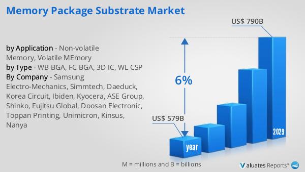
The global semiconductor market, valued at approximately $579 billion in 2022, is anticipated to reach around $790 billion by 2029, reflecting a compound annual growth rate (CAGR) of 6% over the forecast period. This growth trajectory underscores the increasing demand for semiconductors across various industries, driven by technological advancements and the proliferation of electronic devices. The semiconductor market's expansion is fueled by the rising adoption of technologies such as artificial intelligence, the Internet of Things (IoT), and 5G, which require advanced semiconductor solutions. As industries continue to embrace digital transformation, the demand for semiconductors is expected to grow, supporting the development of innovative products and services. The Global Memory Package Substrate Market plays a pivotal role in this growth, providing the necessary substrates for memory packaging, which are essential components in semiconductor devices. The market's evolution is characterized by the continuous development of new materials and manufacturing processes, enhancing the performance and efficiency of memory package substrates. As the semiconductor industry continues to evolve, the Global Memory Package Substrate Market is poised to contribute significantly to its growth, supporting the development of cutting-edge technologies and applications.
| Report Metric | Details |
| Report Name | Memory Package Substrate Market |
| Accounted market size in year | US$ 579 billion |
| Forecasted market size in 2029 | US$ 790 billion |
| CAGR | 6% |
| Base Year | year |
| Forecasted years | 2025 - 2029 |
| by Type |
|
| by Application |
|
| Production by Region |
|
| Consumption by Region |
|
| By Company | Samsung Electro-Mechanics, Simmtech, Daeduck, Korea Circuit, Ibiden, Kyocera, ASE Group, Shinko, Fujitsu Global, Doosan Electronic, Toppan Printing, Unimicron, Kinsus, Nanya |
| Forecast units | USD million in value |
| Report coverage | Revenue and volume forecast, company share, competitive landscape, growth factors and trends |


