What is Global Electron Beam Defect Inspection and Measurement Equipment Market?
The Global Electron Beam Defect Inspection and Measurement Equipment Market is a specialized sector within the semiconductor industry that focuses on the use of electron beam technology to identify and measure defects in semiconductor wafers and masks. This market is crucial for ensuring the quality and reliability of semiconductor devices, which are foundational to modern electronics. Electron beam technology offers high precision and resolution, making it ideal for detecting minute defects that could affect the performance of semiconductor components. The market encompasses various equipment types, including defect inspection systems and metrology tools, each designed to address specific aspects of semiconductor manufacturing. As the demand for smaller, more powerful, and efficient electronic devices grows, the need for advanced inspection and measurement solutions becomes increasingly important. This market is driven by technological advancements, increasing complexity in semiconductor designs, and the need for stringent quality control measures. The growth of this market is also influenced by regional developments, particularly in countries like China, where advancements in electron beam technology and supportive policies are contributing to market expansion. Overall, the Global Electron Beam Defect Inspection and Measurement Equipment Market plays a vital role in the semiconductor industry by ensuring the production of high-quality, reliable electronic components.
Electron Beam Defect Inspection Equipment, Electron Beam Metrology Equipment in the Global Electron Beam Defect Inspection and Measurement Equipment Market:
Electron Beam Defect Inspection Equipment and Electron Beam Metrology Equipment are integral components of the Global Electron Beam Defect Inspection and Measurement Equipment Market. These tools are essential for maintaining the quality and performance of semiconductor devices. Electron Beam Defect Inspection Equipment is designed to detect and analyze defects on semiconductor wafers and masks. These defects can include particles, pattern defects, and other anomalies that could impact the functionality of the final product. The equipment uses a focused beam of electrons to scan the surface of the wafer or mask, capturing high-resolution images that reveal even the smallest defects. This level of precision is crucial for identifying issues that might be missed by other inspection methods. On the other hand, Electron Beam Metrology Equipment is used to measure the dimensions and properties of semiconductor features with high accuracy. This equipment is vital for ensuring that the manufacturing process adheres to the strict specifications required for advanced semiconductor devices. By providing precise measurements, electron beam metrology tools help manufacturers maintain consistency and quality across production batches. The integration of these technologies into the semiconductor manufacturing process allows for early detection and correction of defects, reducing the risk of costly failures and improving overall yield. As semiconductor devices become more complex, with smaller feature sizes and higher performance requirements, the demand for advanced inspection and metrology solutions continues to grow. This demand is further fueled by the increasing adoption of technologies such as artificial intelligence, the Internet of Things, and 5G, which require highly reliable and efficient semiconductor components. The Global Electron Beam Defect Inspection and Measurement Equipment Market is poised for significant growth as manufacturers seek to enhance their quality control processes and meet the evolving demands of the electronics industry.
Wafer, Mask in the Global Electron Beam Defect Inspection and Measurement Equipment Market:
The usage of Global Electron Beam Defect Inspection and Measurement Equipment Market in the areas of wafers and masks is critical for the semiconductor manufacturing process. Wafers are thin slices of semiconductor material, such as silicon, used as the substrate for fabricating integrated circuits. The quality of these wafers is paramount, as any defects can lead to failures in the final electronic devices. Electron beam defect inspection equipment is employed to meticulously scan the surface of wafers, identifying any particles, scratches, or pattern defects that could compromise the integrity of the circuits. This inspection process is essential for ensuring that only wafers meeting the highest quality standards proceed to the next stages of production. Similarly, masks, which are used in photolithography to transfer circuit patterns onto wafers, must be free of defects to ensure accurate patterning. Electron beam inspection tools are used to examine masks for defects that could lead to misalignment or incomplete pattern transfer. By detecting and addressing these issues early in the manufacturing process, manufacturers can prevent costly errors and improve the yield of functional devices. The precision and accuracy of electron beam technology make it an invaluable tool for maintaining the quality of both wafers and masks. As the semiconductor industry continues to push the boundaries of miniaturization and performance, the need for advanced inspection and measurement solutions becomes even more critical. The Global Electron Beam Defect Inspection and Measurement Equipment Market provides the tools necessary to meet these challenges, enabling manufacturers to produce high-quality, reliable semiconductor components that power the latest technological innovations.
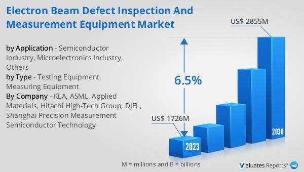
Global Electron Beam Defect Inspection and Measurement Equipment Market Outlook:
The global market for Electron Beam Defect Inspection and Measurement Equipment was valued at $3,126 million in 2024 and is anticipated to grow to a revised size of $4,946 million by 2031, reflecting a compound annual growth rate (CAGR) of 6.7% during the forecast period. This growth is driven by several factors, including advancements in electron beam technology, particularly in China, where the emergence of cost advantages and strengthened policy support are contributing to market expansion. By 2031, it is expected that China's share of the market will reach 4.9%. The increasing complexity of semiconductor devices and the demand for higher quality standards are also fueling the growth of this market. As manufacturers strive to produce smaller, more powerful, and efficient electronic components, the need for precise inspection and measurement solutions becomes paramount. The Global Electron Beam Defect Inspection and Measurement Equipment Market is well-positioned to meet these demands, providing the tools necessary to ensure the quality and reliability of semiconductor devices. This market outlook highlights the significant opportunities for growth and innovation within the industry, driven by technological advancements and the increasing importance of quality control in semiconductor manufacturing.
| Report Metric | Details |
| Report Name | Electron Beam Defect Inspection and Measurement Equipment Market |
| Accounted market size in year | US$ 3126 million |
| Forecasted market size in 2031 | US$ 4946 million |
| CAGR | 6.7% |
| Base Year | year |
| Forecasted years | 2025 - 2031 |
| Segment by Type |
|
| Segment by Application |
|
| Production by Region |
|
| Consumption by Region |
|
| By Company | Applied Materials, Hitachi High-Tech, ASML, KLA, Advantest, Holon Co., Ltd, Wuhan Jingce Electronic Group, DJEL, Wellrun Microelectronics, Suzhou Siscantech, Beijing Hengren, Suzhou AISTech, Huayan Xince Semiconductor (Suzhou) Co., Ltd |
| Forecast units | USD million in value |
| Report coverage | Revenue and volume forecast, company share, competitive landscape, growth factors and trends |