What is Global ArF Immersion Photoresist Market?
The Global ArF Immersion Photoresist Market is a specialized segment within the semiconductor industry, focusing on advanced photolithography processes. ArF, or Argon Fluoride, immersion photoresists are crucial materials used in the production of microchips. These photoresists are designed to work with ArF excimer lasers, which emit light at a wavelength of 193 nanometers. This technology is essential for creating the intricate patterns on silicon wafers that form the basis of integrated circuits. The immersion technique involves using a liquid medium to enhance the resolution of the photolithography process, allowing for the production of smaller and more complex semiconductor devices. This market is driven by the increasing demand for high-performance and miniaturized electronic devices, such as smartphones, tablets, and other consumer electronics. As technology continues to advance, the need for more sophisticated and efficient photoresists grows, making the Global ArF Immersion Photoresist Market a critical component of the semiconductor manufacturing industry. The market is characterized by rapid technological advancements and a high level of competition among key players striving to develop innovative solutions to meet the evolving needs of the semiconductor industry.
Positive Photoresists, Negative Photoresists in the Global ArF Immersion Photoresist Market:
Positive and negative photoresists are two fundamental types of materials used in the Global ArF Immersion Photoresist Market, each serving distinct roles in the photolithography process. Positive photoresists are designed to become soluble when exposed to light, allowing the exposed areas to be washed away during the development process. This results in a pattern that matches the mask used during exposure. Positive photoresists are favored for their high resolution and ability to produce fine patterns, making them ideal for applications requiring precision and detail. They are commonly used in the production of advanced microchips and integrated circuits, where intricate designs are essential for functionality and performance. On the other hand, negative photoresists work in the opposite manner. When exposed to light, they become insoluble, meaning the unexposed areas are removed during development. This results in a pattern that is the inverse of the mask. Negative photoresists are known for their robustness and ability to create thicker layers, which can be advantageous in certain applications where durability and structural integrity are critical. They are often used in the production of MEMS (Micro-Electro-Mechanical Systems) and other applications where thicker resist layers are beneficial. The choice between positive and negative photoresists depends on the specific requirements of the manufacturing process, including the desired resolution, pattern complexity, and material properties. In the context of the Global ArF Immersion Photoresist Market, both types of photoresists play a vital role in enabling the production of cutting-edge semiconductor devices. As the demand for smaller, faster, and more efficient electronic devices continues to grow, the development and optimization of both positive and negative photoresists remain a key focus for manufacturers. Companies in this market are continually investing in research and development to enhance the performance and capabilities of these materials, ensuring they can meet the ever-evolving needs of the semiconductor industry. The competition among manufacturers is intense, with each striving to offer products that provide superior resolution, sensitivity, and process compatibility. This drive for innovation is essential for maintaining a competitive edge in the rapidly advancing field of semiconductor manufacturing. As technology progresses, the distinction between positive and negative photoresists may become less pronounced, with hybrid solutions emerging to offer the best of both worlds. However, for now, both types of photoresists remain indispensable tools in the arsenal of semiconductor manufacturers, each offering unique advantages that cater to different aspects of the photolithography process. The ongoing advancements in photoresist technology are crucial for supporting the continued growth and evolution of the Global ArF Immersion Photoresist Market, ensuring that it can keep pace with the demands of modern electronics and the ever-increasing complexity of semiconductor devices.
Logic IC, Memory IC, Others in the Global ArF Immersion Photoresist Market:
The Global ArF Immersion Photoresist Market plays a crucial role in the production of various types of integrated circuits (ICs), including Logic ICs, Memory ICs, and others. Logic ICs are the building blocks of digital circuits, responsible for processing information and executing instructions in electronic devices. The demand for high-performance Logic ICs is driven by the need for faster and more efficient computing power in applications such as smartphones, computers, and data centers. ArF immersion photoresists are essential in the manufacturing of Logic ICs, as they enable the creation of intricate patterns on silicon wafers with high precision and resolution. This allows for the production of smaller and more powerful Logic ICs, meeting the demands of modern technology. Memory ICs, on the other hand, are used to store data in electronic devices. The demand for Memory ICs is fueled by the increasing need for data storage in applications such as cloud computing, artificial intelligence, and the Internet of Things (IoT). ArF immersion photoresists are critical in the production of Memory ICs, as they enable the creation of high-density memory cells with precise patterning and alignment. This ensures that Memory ICs can store more data in a smaller footprint, meeting the growing demand for data storage in today's digital world. In addition to Logic and Memory ICs, the Global ArF Immersion Photoresist Market also serves other applications, such as microprocessors, sensors, and optoelectronic devices. These applications require advanced photolithography techniques to create complex patterns and structures on semiconductor wafers. ArF immersion photoresists are essential in these applications, as they provide the necessary resolution and precision to produce high-quality semiconductor devices. The versatility and adaptability of ArF immersion photoresists make them indispensable in the production of a wide range of semiconductor devices, supporting the continued growth and innovation in the electronics industry. As technology continues to advance, the demand for more sophisticated and efficient semiconductor devices will only increase, driving the need for advanced photolithography solutions like ArF immersion photoresists. The Global ArF Immersion Photoresist Market is poised to play a critical role in meeting these demands, ensuring that the semiconductor industry can continue to innovate and evolve in response to the ever-changing needs of the digital world.
Global ArF Immersion Photoresist Market Outlook:
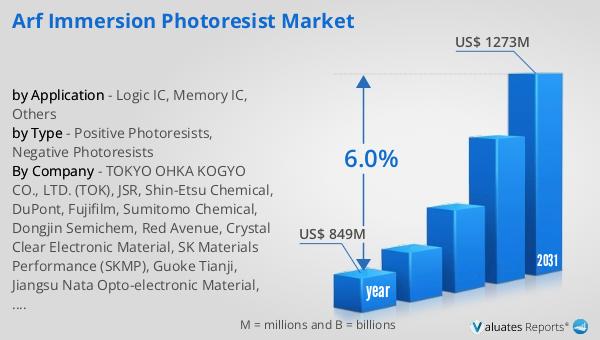
The global market for ArF Immersion Photoresist was valued at $849 million in 2024 and is anticipated to grow to a revised size of $1,273 million by 2031, reflecting a compound annual growth rate (CAGR) of 6.0% during the forecast period. The market is dominated by the top four players, who collectively hold a share exceeding 85%. Key foundries in this sector include TSMC, Samsung Foundry, GlobalFoundries, United Microelectronics Corporation (UMC), SMIC, Tower Semiconductor, PSMC, VIS (Vanguard International Semiconductor), Hua Hong Semiconductor, and HLMC. In 2023, the global foundries market size was valued at $113.1 billion and is projected to reach $277.9 billion by 2030. Similarly, the global IDM-only wafer fabrication market was valued at $138.6 billion in 2023 and is expected to grow to $228.6 billion by 2030. These figures highlight the significant growth potential and importance of the ArF Immersion Photoresist Market within the broader semiconductor industry. The market's expansion is driven by the increasing demand for advanced semiconductor devices and the continuous advancements in photolithography technology. As the semiconductor industry continues to evolve, the Global ArF Immersion Photoresist Market is expected to play a pivotal role in supporting the development and production of cutting-edge electronic devices.
| Report Metric | Details |
| Report Name | ArF Immersion Photoresist Market |
| Accounted market size in year | US$ 849 million |
| Forecasted market size in 2031 | US$ 1273 million |
| CAGR | 6.0% |
| Base Year | year |
| Forecasted years | 2025 - 2031 |
| by Type |
|
| by Application |
|
| Production by Region |
|
| Consumption by Region |
|
| By Company | TOKYO OHKA KOGYO CO., LTD. (TOK), JSR, Shin-Etsu Chemical, DuPont, Fujifilm, Sumitomo Chemical, Dongjin Semichem, Red Avenue, Crystal Clear Electronic Material, SK Materials Performance (SKMP), Guoke Tianji, Jiangsu Nata Opto-electronic Material, Xiamen Hengkun New Material Technology, Zhuhai Cornerstone Technologies, SINEVA |
| Forecast units | USD million in value |
| Report coverage | Revenue and volume forecast, company share, competitive landscape, growth factors and trends |