What is Global Photosensitive Materials for Photoresists Market?
The global market for photosensitive materials for photoresists is a specialized segment within the broader semiconductor industry. These materials are crucial in the photolithography process, which is a key step in semiconductor manufacturing. Photolithography involves transferring a pattern from a photomask to the surface of a substrate, typically a silicon wafer, using light. Photosensitive materials, or photoresists, are applied to the wafer and exposed to light, which causes a chemical change in the material. This change allows for the selective removal of either the exposed or unexposed areas, depending on whether a positive or negative photoresist is used. The global market for these materials was valued at US$ 156 million in 2024 and is expected to grow significantly, reaching US$ 229 million by 2031. This growth is driven by the increasing demand for advanced semiconductor devices, which require more sophisticated photolithography techniques and materials. As the semiconductor industry continues to evolve, the demand for high-performance photoresists and their associated materials is expected to rise, supporting the development of smaller, faster, and more efficient electronic devices. The market's expansion is also influenced by technological advancements and the growing complexity of semiconductor manufacturing processes.
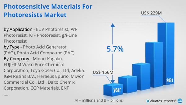
Photo Acid Generator (PAG), Photo Acid Compound (PAC) in the Global Photosensitive Materials for Photoresists Market:
Photo Acid Generators (PAGs) and Photo Acid Compounds (PACs) are integral components of the global photosensitive materials for photoresists market. These compounds play a crucial role in the photolithography process, which is essential for semiconductor manufacturing. PAGs are chemical compounds that release acid upon exposure to light, typically ultraviolet (UV) light. This acid generation is a key step in the photolithographic process, as it initiates a chemical reaction that alters the solubility of the photoresist material. The acid generated by PAGs catalyzes the deprotection of the photoresist polymer, making it soluble in a developer solution. This solubility change allows for the selective removal of either the exposed or unexposed areas of the photoresist, depending on whether a positive or negative photoresist is used. PACs, on the other hand, are compounds that contain an acid group that is protected by a photolabile protecting group. Upon exposure to light, the protecting group is cleaved, releasing the acid. This acid then catalyzes the deprotection of the photoresist polymer, similar to the action of PAGs. The choice between PAGs and PACs depends on the specific requirements of the photolithography process, including the desired resolution, sensitivity, and compatibility with other materials. The development of advanced PAGs and PACs has been driven by the need for higher resolution and sensitivity in photolithography, as semiconductor devices continue to shrink in size. These compounds are designed to generate strong acids with high quantum efficiency, ensuring efficient deprotection of the photoresist polymer. Additionally, they are engineered to minimize the generation of volatile byproducts, which can cause defects in the final semiconductor device. The global market for PAGs and PACs is influenced by several factors, including the increasing demand for advanced semiconductor devices, the development of new photolithography techniques, and the growing complexity of semiconductor manufacturing processes. As the semiconductor industry continues to evolve, the demand for high-performance PAGs and PACs is expected to rise, supporting the development of smaller, faster, and more efficient electronic devices. The market's expansion is also driven by technological advancements and the increasing complexity of semiconductor manufacturing processes. In conclusion, PAGs and PACs are essential components of the global photosensitive materials for photoresists market. These compounds play a critical role in the photolithography process, enabling the production of advanced semiconductor devices. The development of high-performance PAGs and PACs is driven by the need for higher resolution and sensitivity in photolithography, as well as the increasing complexity of semiconductor manufacturing processes. As the semiconductor industry continues to evolve, the demand for these compounds is expected to rise, supporting the development of smaller, faster, and more efficient electronic devices.
EUV Photoresist, ArF Photoresist, KrF Photoresist, g/i-Line Photoresist in the Global Photosensitive Materials for Photoresists Market:
The global photosensitive materials for photoresists market finds extensive usage in various types of photoresists, including EUV (Extreme Ultraviolet) Photoresist, ArF (Argon Fluoride) Photoresist, KrF (Krypton Fluoride) Photoresist, and g/i-Line Photoresist. Each of these photoresists serves a specific purpose in the semiconductor manufacturing process, catering to different technological requirements and advancements. EUV Photoresist is at the forefront of photolithography technology, designed for use with extreme ultraviolet light sources. This type of photoresist is crucial for producing the smallest and most advanced semiconductor devices, as it allows for the creation of extremely fine patterns on silicon wafers. The development of EUV photoresists is driven by the need for higher resolution and precision in semiconductor manufacturing, enabling the production of smaller, faster, and more efficient electronic devices. ArF Photoresist, on the other hand, is used in conjunction with argon fluoride lasers, which emit light at a wavelength of 193 nanometers. This type of photoresist is widely used in the production of advanced semiconductor devices, as it offers a good balance between resolution and sensitivity. ArF photoresists are essential for producing devices with feature sizes in the range of 45 to 65 nanometers, making them suitable for a wide range of applications in the semiconductor industry. KrF Photoresist is designed for use with krypton fluoride lasers, which emit light at a wavelength of 248 nanometers. This type of photoresist is commonly used in the production of semiconductor devices with feature sizes in the range of 130 to 250 nanometers. KrF photoresists offer good resolution and sensitivity, making them suitable for a wide range of applications in the semiconductor industry. Finally, g/i-Line Photoresist is used in conjunction with g-line (436 nanometers) and i-line (365 nanometers) light sources. This type of photoresist is typically used in the production of semiconductor devices with larger feature sizes, in the range of 350 to 500 nanometers. g/i-Line photoresists are widely used in the production of less advanced semiconductor devices, as well as in applications where cost is a significant factor. In conclusion, the global photosensitive materials for photoresists market plays a crucial role in the production of semiconductor devices, catering to a wide range of technological requirements and advancements. Each type of photoresist, including EUV, ArF, KrF, and g/i-Line, serves a specific purpose in the semiconductor manufacturing process, enabling the production of devices with varying feature sizes and complexities. As the semiconductor industry continues to evolve, the demand for high-performance photoresists and their associated materials is expected to rise, supporting the development of smaller, faster, and more efficient electronic devices.
Global Photosensitive Materials for Photoresists Market Outlook:
In 2024, the global market for photosensitive materials used in photoresists was valued at approximately US$ 156 million. This market is anticipated to expand significantly, reaching an estimated value of US$ 229 million by 2031, with a compound annual growth rate (CAGR) of 5.7% during the forecast period. This growth is indicative of the increasing demand for advanced semiconductor devices, which necessitate more sophisticated photolithography techniques and materials. In parallel, the global semiconductor market was valued at US$ 526.8 billion in 2023 and is projected to grow to US$ 780.7 billion by 2030. This growth trajectory underscores the expanding role of semiconductors in various industries, driven by technological advancements and the proliferation of electronic devices. Furthermore, the global semiconductor manufacturing wafer fabrication market is expected to grow from US$ 251.7 billion in 2023 to US$ 506.5 billion by 2030, reflecting a robust CAGR of 40.49% during the forecast period. This substantial growth highlights the increasing complexity and sophistication of semiconductor manufacturing processes, which in turn drives the demand for high-performance photosensitive materials for photoresists. As the semiconductor industry continues to evolve, the market for these materials is poised for significant expansion, supporting the development of smaller, faster, and more efficient electronic devices.
| Report Metric | Details |
| Report Name | Photosensitive Materials for Photoresists Market |
| Accounted market size in year | US$ 156 million |
| Forecasted market size in 2031 | US$ 229 million |
| CAGR | 5.7% |
| Base Year | year |
| Forecasted years | 2025 - 2031 |
| by Type |
|
| by Application |
|
| Production by Region |
|
| Consumption by Region |
|
| By Company | Midori Kagaku, FUJIFILM Wako Pure Chemical Corporation, Toyo Gosei Co., Ltd, Adeka, IGM Resins B.V., Heraeus Epurio, Miwon Commercial Co., Ltd., Daito Chemix Corporation, CGP Materials, ENF Technology, NC Chem, TAKOMA TECHNOLOGY CORPORATION, Xuzhou B & C Chemical, Changzhou Tronly New Electronic Materials, Tianjin Jiuri New Material, Suzhou Weimas |
| Forecast units | USD million in value |
| Report coverage | Revenue and volume forecast, company share, competitive landscape, growth factors and trends |


