What is Global MEMS Microbolometer Market?
The Global MEMS Microbolometer Market is a fascinating segment of the technology industry that focuses on the development and application of micro-electromechanical systems (MEMS) for thermal imaging. Microbolometers are a type of sensor used in thermal cameras to detect infrared radiation, which is invisible to the naked eye. These sensors are crucial for converting thermal energy into an electronic signal, allowing for the visualization of heat patterns. The market for MEMS microbolometers is driven by their increasing use in various applications, such as surveillance, firefighting, and industrial inspection, due to their ability to provide clear thermal images without the need for cooling. This technology is particularly valued for its compact size, low power consumption, and cost-effectiveness compared to traditional thermal imaging solutions. As industries continue to recognize the benefits of thermal imaging for safety, security, and efficiency, the demand for MEMS microbolometers is expected to grow. The market is characterized by continuous innovation, with manufacturers striving to improve the sensitivity, resolution, and affordability of these sensors to meet the diverse needs of different sectors. Overall, the Global MEMS Microbolometer Market represents a dynamic and evolving field with significant potential for future growth and development.
Pixel Size 17μm, Pixel Size 12μm, Pixel Size 10μm, Others in the Global MEMS Microbolometer Market:
In the Global MEMS Microbolometer Market, pixel size plays a crucial role in determining the performance and application of thermal imaging sensors. Pixel size refers to the dimensions of each individual sensor element on the microbolometer array, and it directly impacts the resolution and sensitivity of the thermal image produced. Smaller pixel sizes generally allow for higher resolution images, which can be critical in applications requiring detailed thermal analysis. The most common pixel sizes in the market are 17μm, 12μm, and 10μm, each offering distinct advantages and trade-offs. The 17μm pixel size is often used in applications where cost-effectiveness is a priority, as it provides a good balance between resolution and affordability. This pixel size is suitable for general-purpose thermal imaging tasks, such as building inspections and basic surveillance, where ultra-high resolution is not necessary. On the other hand, the 12μm pixel size offers improved resolution and sensitivity, making it ideal for more demanding applications like advanced surveillance, precision agriculture, and medical diagnostics. The smaller pixel size allows for more detailed thermal images, which can be crucial in identifying subtle temperature variations and anomalies. The 10μm pixel size represents the cutting edge of MEMS microbolometer technology, providing the highest resolution and sensitivity available. This pixel size is typically used in specialized applications that require the utmost precision, such as scientific research, high-end security systems, and aerospace. The smaller pixel size enables the detection of minute temperature differences, which can be critical in environments where accuracy is paramount. Additionally, the trend towards smaller pixel sizes is driven by the ongoing miniaturization of electronic components and the demand for more compact and portable thermal imaging devices. As technology advances, manufacturers are continually working to reduce pixel sizes while maintaining or even enhancing the performance of the sensors. This progress is essential for expanding the range of applications for MEMS microbolometers and meeting the evolving needs of various industries. Furthermore, the development of smaller pixel sizes is often accompanied by improvements in other aspects of sensor performance, such as faster response times and lower power consumption. These enhancements contribute to the overall efficiency and effectiveness of thermal imaging systems, making them more attractive to a wider range of users. In summary, the choice of pixel size in the Global MEMS Microbolometer Market is a critical factor that influences the capabilities and applications of thermal imaging sensors. Each pixel size offers unique benefits, and the ongoing trend towards smaller pixels is driving innovation and expanding the potential uses of this technology. As the market continues to evolve, the development of even smaller pixel sizes and further improvements in sensor performance are likely to play a key role in shaping the future of thermal imaging.
Military, Civilian in the Global MEMS Microbolometer Market:
The Global MEMS Microbolometer Market finds significant usage in both military and civilian applications, each with distinct requirements and benefits. In the military sector, MEMS microbolometers are primarily used for surveillance, target acquisition, and reconnaissance. The ability to detect heat signatures without the need for visible light makes these sensors invaluable for night operations and in environments with poor visibility. Thermal imaging allows military personnel to identify potential threats, track movements, and navigate challenging terrains, providing a strategic advantage in various combat scenarios. The compact size and low power consumption of MEMS microbolometers make them ideal for integration into portable devices, such as handheld thermal cameras and weapon sights, enhancing the mobility and effectiveness of military forces. Additionally, these sensors are used in unmanned aerial vehicles (UAVs) and other remote sensing platforms, enabling real-time thermal imaging over large areas. In civilian applications, MEMS microbolometers are widely used for safety, security, and efficiency purposes. In the field of firefighting, thermal cameras equipped with these sensors help firefighters see through smoke, locate hotspots, and rescue individuals trapped in burning buildings. The ability to visualize heat patterns is crucial for assessing fire dynamics and making informed decisions in life-threatening situations. In the realm of security, thermal imaging is employed for perimeter surveillance, intrusion detection, and monitoring critical infrastructure. The ability to detect heat signatures in complete darkness or adverse weather conditions enhances the effectiveness of security systems, providing an additional layer of protection for sensitive areas. MEMS microbolometers are also used in industrial applications for equipment monitoring and predictive maintenance. By detecting abnormal heat patterns, these sensors can identify potential equipment failures before they occur, reducing downtime and maintenance costs. In the medical field, thermal imaging is used for non-invasive diagnostics, such as detecting inflammation, monitoring blood flow, and assessing skin conditions. The ability to visualize temperature variations on the human body provides valuable insights for medical professionals, aiding in the diagnosis and treatment of various conditions. Furthermore, MEMS microbolometers are increasingly used in consumer electronics, such as smartphones and wearable devices, for applications like facial recognition and augmented reality. The integration of thermal imaging capabilities into everyday devices opens up new possibilities for enhancing user experiences and improving functionality. Overall, the Global MEMS Microbolometer Market plays a vital role in both military and civilian sectors, offering a wide range of applications that enhance safety, security, and efficiency. The versatility and effectiveness of thermal imaging technology continue to drive its adoption across various industries, highlighting the importance of ongoing innovation and development in this field.
Global MEMS Microbolometer Market Outlook:
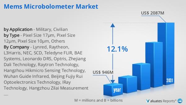
The global market for MEMS Microbolometer was valued at approximately $946 million in 2024, and it is anticipated to expand significantly, reaching an estimated size of $2,087 million by 2031. This growth trajectory represents a compound annual growth rate (CAGR) of 12.1% over the forecast period. The robust growth of this market can be attributed to several factors, including the increasing demand for thermal imaging solutions across various industries. As more sectors recognize the benefits of thermal imaging for applications such as surveillance, firefighting, and industrial inspection, the demand for MEMS microbolometers is expected to rise. The market's expansion is also driven by technological advancements that enhance the performance and affordability of these sensors, making them more accessible to a broader range of users. Additionally, the trend towards miniaturization and the development of smaller pixel sizes contribute to the market's growth by enabling the integration of thermal imaging capabilities into more compact and portable devices. As the market continues to evolve, manufacturers are likely to focus on further improving the sensitivity, resolution, and cost-effectiveness of MEMS microbolometers to meet the diverse needs of different sectors. Overall, the Global MEMS Microbolometer Market is poised for significant growth, driven by increasing demand, technological advancements, and the expanding range of applications for thermal imaging technology.
| Report Metric | Details |
| Report Name | MEMS Microbolometer Market |
| Accounted market size in year | US$ 946 million |
| Forecasted market size in 2031 | US$ 2087 million |
| CAGR | 12.1% |
| Base Year | year |
| Forecasted years | 2025 - 2031 |
| by Type |
|
| by Application |
|
| Production by Region |
|
| Consumption by Region |
|
| By Company | Lynred, Raytheon, L3Harris, NEC, SCD, Teledyne FLIR, BAE Systems, Leonardo DRS, Optris, Zhejiang Dali Technology, Raytron Technology, Hangzhou Hikmicro Sensing Technology, Wuhan Guide Infrared, Beijing Fujiy Rui Optoelectronics Technology, IRay Technology, Hangzhou Zilai Measurement and Control Technology |
| Forecast units | USD million in value |
| Report coverage | Revenue and volume forecast, company share, competitive landscape, growth factors and trends |


