What is Global Gallium Nitride (GaN) Wafer Foundry Market?
The Global Gallium Nitride (GaN) Wafer Foundry Market is a specialized segment within the semiconductor industry that focuses on the production and supply of GaN wafers. These wafers are essential components used in the manufacturing of high-performance electronic devices. GaN is a semiconductor material known for its superior properties, such as high electron mobility, high breakdown voltage, and thermal stability, making it ideal for applications in power electronics and radio frequency (RF) devices. The market is driven by the increasing demand for energy-efficient and high-frequency electronic devices across various industries, including telecommunications, automotive, and consumer electronics. As technology advances, the need for smaller, faster, and more efficient devices continues to grow, propelling the demand for GaN wafers. Foundries specializing in GaN wafer production play a crucial role in meeting this demand by providing high-quality wafers to device manufacturers. The market is characterized by continuous innovation and development, with companies investing in research and development to enhance the performance and efficiency of GaN wafers. As a result, the Global GaN Wafer Foundry Market is poised for significant growth in the coming years, driven by technological advancements and increasing adoption of GaN-based devices.
in the Global Gallium Nitride (GaN) Wafer Foundry Market:
In the Global Gallium Nitride (GaN) Wafer Foundry Market, various types of GaN wafers are utilized by different customers, each catering to specific applications and requirements. The primary types of GaN wafers include GaN-on-Silicon (GaN-on-Si), GaN-on-Silicon Carbide (GaN-on-SiC), and GaN-on-Sapphire. GaN-on-Si wafers are popular due to their cost-effectiveness and compatibility with existing silicon-based manufacturing processes. They are widely used in power electronics applications, where cost efficiency and scalability are crucial. GaN-on-SiC wafers, on the other hand, offer superior thermal conductivity and higher power density, making them ideal for high-power and high-frequency applications, such as RF amplifiers and radar systems. GaN-on-Sapphire wafers are known for their excellent thermal stability and are often used in optoelectronic devices, including LEDs and laser diodes. Each type of GaN wafer has its unique advantages and limitations, and the choice of wafer type depends on the specific requirements of the application and the desired performance characteristics. Customers in the telecommunications industry, for example, may prefer GaN-on-SiC wafers for their high-frequency and high-power capabilities, while those in the consumer electronics sector may opt for GaN-on-Si wafers for their cost-effectiveness and compatibility with existing manufacturing processes. The automotive industry, which is increasingly adopting GaN technology for electric vehicles and advanced driver-assistance systems, may utilize a combination of GaN-on-Si and GaN-on-SiC wafers to achieve the desired balance between performance and cost. In addition to the primary types of GaN wafers, there are also variations in wafer size and thickness, which can impact the performance and cost of the final device. Larger wafers, for example, can increase production efficiency and reduce costs, while thinner wafers may offer improved thermal performance and device reliability. As the demand for GaN-based devices continues to grow, foundries are investing in advanced manufacturing technologies and processes to produce high-quality GaN wafers that meet the evolving needs of their customers. This includes the development of new wafer substrates, such as GaN-on-GaN, which offer the potential for even higher performance and efficiency. The choice of GaN wafer type and specifications is a critical decision for customers, as it can significantly impact the performance, cost, and reliability of the final device. As a result, customers often work closely with foundries to select the optimal wafer type and specifications for their specific applications. This collaborative approach ensures that the GaN wafers meet the desired performance characteristics and are compatible with the customer's manufacturing processes. Overall, the Global GaN Wafer Foundry Market is characterized by a diverse range of wafer types and specifications, each catering to the unique needs of different customers and applications. As technology continues to advance and the demand for GaN-based devices grows, the market is expected to see further innovation and development in GaN wafer types and manufacturing processes.
GaN Power Devices, GaN RF Devices in the Global Gallium Nitride (GaN) Wafer Foundry Market:
The Global Gallium Nitride (GaN) Wafer Foundry Market plays a pivotal role in the development and production of GaN power devices and GaN RF devices, both of which are critical components in modern electronic systems. GaN power devices are used in a wide range of applications, including power converters, inverters, and motor drives, where they offer significant advantages over traditional silicon-based devices. GaN power devices are known for their high efficiency, fast switching speeds, and compact size, making them ideal for applications that require high power density and energy efficiency. In power converters, for example, GaN devices can reduce energy losses and improve overall system efficiency, leading to lower energy consumption and reduced operating costs. Similarly, in motor drives, GaN devices can enhance performance and reliability by providing faster and more precise control of motor speed and torque. The automotive industry, in particular, is increasingly adopting GaN power devices for electric vehicles and hybrid electric vehicles, where they contribute to improved energy efficiency and extended driving range. GaN RF devices, on the other hand, are used in high-frequency applications, such as wireless communication systems, radar systems, and satellite communication. GaN RF devices offer superior performance in terms of power output, efficiency, and linearity, making them ideal for applications that require high-frequency and high-power operation. In wireless communication systems, for example, GaN RF devices can enhance signal quality and coverage, enabling faster data transmission and improved network performance. In radar systems, GaN RF devices can provide higher resolution and longer detection range, improving the accuracy and reliability of target detection and tracking. The defense and aerospace industries are among the key adopters of GaN RF devices, where they are used in advanced radar and communication systems for military and space applications. The Global GaN Wafer Foundry Market is instrumental in supporting the development and production of these high-performance GaN devices by providing high-quality GaN wafers that meet the stringent requirements of these applications. Foundries specializing in GaN wafer production work closely with device manufacturers to ensure that the wafers meet the desired performance characteristics and are compatible with the manufacturing processes. This collaboration is essential for achieving the high levels of performance and reliability required in GaN power and RF devices. As the demand for GaN-based devices continues to grow, the Global GaN Wafer Foundry Market is expected to see further innovation and development in wafer manufacturing technologies and processes. This includes the development of new wafer substrates and advanced manufacturing techniques that can enhance the performance and efficiency of GaN devices. Overall, the Global GaN Wafer Foundry Market is a critical enabler of the GaN power and RF device markets, providing the high-quality wafers needed to support the development and production of these advanced electronic components.
Global Gallium Nitride (GaN) Wafer Foundry Market Outlook:
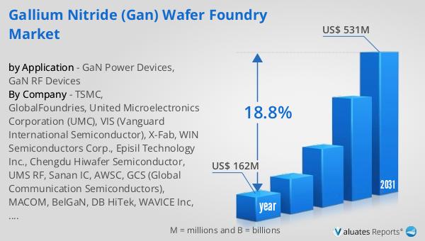
The worldwide market for Gallium Nitride (GaN) Wafer Foundry was estimated to be worth $162 million in 2024. It is anticipated to expand significantly, reaching a revised valuation of $531 million by 2031. This growth trajectory represents a compound annual growth rate (CAGR) of 18.8% over the forecast period. This impressive growth rate underscores the increasing demand for GaN wafers, driven by their superior performance characteristics and the growing adoption of GaN-based devices across various industries. The market's expansion is fueled by the continuous advancements in technology and the rising need for energy-efficient and high-frequency electronic devices. As industries such as telecommunications, automotive, and consumer electronics increasingly adopt GaN technology, the demand for high-quality GaN wafers is expected to rise. Foundries specializing in GaN wafer production are investing in research and development to enhance the performance and efficiency of their products, further driving market growth. The projected growth of the Global GaN Wafer Foundry Market highlights the critical role that GaN technology plays in the development of advanced electronic devices and systems. As the market continues to evolve, it is poised to become a key player in the semiconductor industry, supporting the development and production of high-performance GaN-based devices.
| Report Metric | Details |
| Report Name | Gallium Nitride (GaN) Wafer Foundry Market |
| Accounted market size in year | US$ 162 million |
| Forecasted market size in 2031 | US$ 531 million |
| CAGR | 18.8% |
| Base Year | year |
| Forecasted years | 2025 - 2031 |
| by Application |
|
| Production by Region |
|
| Consumption by Region |
|
| By Company | TSMC, GlobalFoundries, United Microelectronics Corporation (UMC), VIS (Vanguard International Semiconductor), X-Fab, WIN Semiconductors Corp., Episil Technology Inc., Chengdu Hiwafer Semiconductor, UMS RF, Sanan IC, AWSC, GCS (Global Communication Semiconductors), MACOM, BelGaN, DB HiTek, WAVICE Inc, SK keyfoundry, Odyssey Semiconductor, Taiwan-Asia Semiconductor (TASC), Samsung Electronics, by Technology, GaN-on-Si Wafer Foundry, GaN-on-SiC Wafer Foundry |
| Forecast units | USD million in value |
| Report coverage | Revenue and volume forecast, company share, competitive landscape, growth factors and trends |


