What is Global Gallium Nitride (GaN) Wafer Fabrication Market?
The Global Gallium Nitride (GaN) Wafer Fabrication Market is a rapidly evolving sector within the semiconductor industry, primarily driven by the increasing demand for high-performance electronic devices. GaN is a semiconductor material that offers superior properties compared to traditional silicon, such as higher efficiency, faster switching speeds, and greater thermal stability. These characteristics make GaN an ideal choice for a wide range of applications, including power electronics, radio frequency (RF) components, and optoelectronics. The market for GaN wafer fabrication is expanding as industries seek to leverage these advantages to enhance the performance and efficiency of their products. The growth is further fueled by the rising adoption of electric vehicles, renewable energy systems, and advanced communication technologies, all of which require efficient and reliable semiconductor components. As a result, the GaN wafer fabrication market is witnessing significant investments in research and development, as well as the establishment of new manufacturing facilities to meet the growing demand. This dynamic market is poised for continued expansion as technological advancements and increasing applications drive further innovation and adoption of GaN-based solutions.
in the Global Gallium Nitride (GaN) Wafer Fabrication Market:
In the Global Gallium Nitride (GaN) Wafer Fabrication Market, various types of GaN wafers are utilized by different customers, each catering to specific needs and applications. The primary types of GaN wafers include GaN-on-Silicon (GaN-on-Si), GaN-on-Silicon Carbide (GaN-on-SiC), and GaN-on-Sapphire. GaN-on-Si wafers are popular due to their cost-effectiveness and compatibility with existing silicon-based manufacturing processes. This type is widely used in power electronics and RF applications, where cost and integration with existing systems are crucial considerations. GaN-on-SiC wafers, on the other hand, offer superior thermal conductivity and higher power density, making them ideal for high-power and high-frequency applications such as RF amplifiers and radar systems. The enhanced performance of GaN-on-SiC wafers comes at a higher cost, but their ability to handle extreme conditions makes them indispensable in demanding environments. GaN-on-Sapphire wafers are primarily used in optoelectronic applications, such as light-emitting diodes (LEDs) and laser diodes, due to their excellent optical properties. Sapphire substrates provide a lattice match for GaN, resulting in high-quality crystal growth and improved device performance. Each type of GaN wafer offers distinct advantages, allowing customers to select the most suitable option based on their specific requirements and application areas. The choice of wafer type is influenced by factors such as cost, performance, thermal management, and compatibility with existing manufacturing processes. As the GaN wafer fabrication market continues to grow, advancements in material science and manufacturing techniques are expected to further enhance the performance and cost-effectiveness of these wafers, enabling broader adoption across various industries. Customers in the GaN wafer fabrication market include semiconductor manufacturers, electronics companies, and research institutions, all of which are seeking to leverage the unique properties of GaN to develop cutting-edge technologies and products. The diverse range of applications and customer needs drives continuous innovation and competition within the market, fostering the development of new and improved GaN wafer solutions. As a result, the GaN wafer fabrication market is characterized by a dynamic landscape, with ongoing advancements in wafer technology and manufacturing processes shaping the future of the industry.
GaN Power Devices, GaN RF Devices in the Global Gallium Nitride (GaN) Wafer Fabrication Market:
The usage of Global Gallium Nitride (GaN) Wafer Fabrication Market in GaN Power Devices and GaN RF Devices highlights the versatility and efficiency of GaN technology in addressing the demands of modern electronic applications. GaN Power Devices are increasingly being adopted in power conversion and management systems due to their ability to operate at higher voltages and temperatures compared to traditional silicon-based devices. This results in improved energy efficiency, reduced size and weight, and enhanced performance in applications such as power supplies, inverters, and motor drives. The high electron mobility and wide bandgap of GaN enable power devices to switch faster and handle higher power densities, making them ideal for use in electric vehicles, renewable energy systems, and data centers. In GaN RF Devices, the superior frequency response and power handling capabilities of GaN make it a preferred choice for RF amplifiers, transceivers, and radar systems. GaN RF devices offer higher efficiency and linearity, which are critical for maintaining signal integrity and reducing power consumption in wireless communication systems. The ability to operate at higher frequencies and power levels allows GaN RF devices to support advanced communication technologies such as 5G, satellite communications, and military radar systems. The adoption of GaN technology in these areas is driven by the need for higher performance, greater efficiency, and reduced system costs. As the demand for faster and more reliable communication networks continues to grow, GaN RF devices are expected to play a crucial role in enabling the next generation of wireless technologies. The integration of GaN power and RF devices into various applications is facilitated by ongoing advancements in GaN wafer fabrication techniques, which are improving the quality, scalability, and cost-effectiveness of GaN-based solutions. These developments are enabling broader adoption of GaN technology across a wide range of industries, from consumer electronics to aerospace and defense. As a result, the Global GaN Wafer Fabrication Market is poised for significant growth, driven by the increasing demand for high-performance electronic devices and the continuous evolution of GaN technology.
Global Gallium Nitride (GaN) Wafer Fabrication Market Outlook:
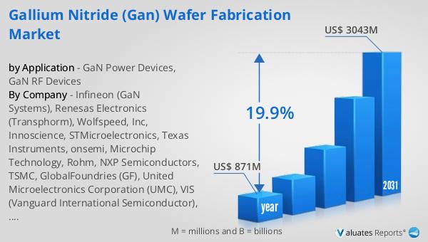
The global market for Gallium Nitride (GaN) Wafer Fabrication was valued at $871 million in 2024 and is anticipated to expand to a revised size of $3,043 million by 2031, reflecting a compound annual growth rate (CAGR) of 19.9% over the forecast period. This impressive growth trajectory underscores the increasing importance and adoption of GaN technology across various industries. The market's expansion is fueled by the rising demand for high-efficiency and high-performance semiconductor devices, which are essential for powering the next generation of electronic applications. As industries continue to seek innovative solutions to enhance the performance and efficiency of their products, GaN wafer fabrication is emerging as a key enabler of technological advancement. The projected growth of the GaN wafer fabrication market highlights the significant investments being made in research and development, as well as the establishment of new manufacturing facilities to meet the growing demand. This dynamic market is characterized by continuous innovation and competition, as companies strive to develop cutting-edge GaN-based solutions that address the evolving needs of their customers. As a result, the GaN wafer fabrication market is poised for continued expansion, driven by the increasing adoption of GaN technology and the ongoing evolution of semiconductor manufacturing processes.
| Report Metric | Details |
| Report Name | Gallium Nitride (GaN) Wafer Fabrication Market |
| Accounted market size in year | US$ 871 million |
| Forecasted market size in 2031 | US$ 3043 million |
| CAGR | 19.9% |
| Base Year | year |
| Forecasted years | 2025 - 2031 |
| by Application |
|
| Production by Region |
|
| Consumption by Region |
|
| By Company | Infineon (GaN Systems), Renesas Electronics (Transphorm), Wolfspeed, Inc, Innoscience, STMicroelectronics, Texas Instruments, onsemi, Microchip Technology, Rohm, NXP Semiconductors, TSMC, GlobalFoundries (GF), United Microelectronics Corporation (UMC), VIS (Vanguard International Semiconductor), X-Fab, WIN Semiconductors Corp., Episil Technology Inc., UMS RF, Sanan IC, Chengdu Hiwafer Semiconductor, Samsung Electronics, BelGaN, DB HiTek, WAVICE Inc, SK keyfoundry, BAE Systems, Odyssey Semiconductor, Taiwan-Asia Semiconductor (TASC), Sumitomo Electric Device Innovations (SEDI) (SCIOCS), Qorvo, Toshiba, Alpha and Omega Semiconductor Limited (AOS), Nexperia, Epistar Corp., CETC 13, CETC 55, China Resources Microelectronics Limited, CorEnergy, Sanan Optoelectronics, Hangzhou Silan Microelectronics, Qingdao Cohenius Microelectronics, Dynax Semiconductor, Guangdong ZIENER Technology, Nuvoton Technology Corporation, Toyoda Gosei, by Technology, GaN Wafer Foundry, GaN Wafer IDM Model |
| Forecast units | USD million in value |
| Report coverage | Revenue and volume forecast, company share, competitive landscape, growth factors and trends |


