What is Global Wafer Backside Protection Film Market?
The Global Wafer Backside Protection Film Market is a specialized segment within the semiconductor industry that focuses on providing protective films for the backside of wafers. These films are crucial during the manufacturing process of semiconductors, as they protect the delicate wafer surfaces from scratches, contamination, and mechanical damage. The protection film is applied to the wafer's backside to ensure that the front side, which contains the intricate circuitry, remains pristine and functional. This market is driven by the increasing demand for semiconductors in various applications, including consumer electronics, automotive, and industrial sectors. As technology advances, the need for more sophisticated and reliable semiconductor components grows, thereby boosting the demand for wafer backside protection films. These films not only enhance the durability and performance of the wafers but also contribute to the overall efficiency of the semiconductor manufacturing process. The market is characterized by continuous innovation, with manufacturers striving to develop films that offer better protection, are easier to apply, and can withstand the rigorous conditions of semiconductor fabrication. As a result, the Global Wafer Backside Protection Film Market plays a vital role in supporting the semiconductor industry's growth and technological advancements.
25μm, 40μm in the Global Wafer Backside Protection Film Market:
In the Global Wafer Backside Protection Film Market, the thickness of the film is a critical factor that influences its performance and suitability for different applications. Two common thicknesses in this market are 25μm and 40μm. The 25μm films are typically used in applications where a thinner protective layer is sufficient to safeguard the wafer's backside. These films are favored for their flexibility and ability to conform to the wafer's surface, providing adequate protection without adding significant bulk. They are particularly useful in applications where space is a constraint, or where the wafers are subjected to less mechanical stress. On the other hand, 40μm films offer a thicker protective layer, which is beneficial in scenarios where the wafers are exposed to harsher conditions or require additional mechanical support. The increased thickness provides enhanced protection against scratches and other forms of physical damage, making them ideal for more demanding applications. The choice between 25μm and 40μm films depends on various factors, including the specific requirements of the semiconductor manufacturing process, the type of wafer being used, and the environmental conditions to which the wafers will be exposed. Manufacturers in the Global Wafer Backside Protection Film Market continuously innovate to improve the performance of these films, ensuring they meet the evolving needs of the semiconductor industry. This includes developing films with improved adhesion properties, resistance to chemicals, and the ability to withstand high temperatures. As the demand for semiconductors continues to grow, driven by advancements in technology and the increasing integration of electronic components in various devices, the need for reliable and effective wafer backside protection films will remain strong. The market for these films is expected to expand as manufacturers seek to enhance the performance and durability of their semiconductor products. In summary, the 25μm and 40μm films play a crucial role in the Global Wafer Backside Protection Film Market, offering different levels of protection to meet the diverse needs of the semiconductor industry.
200mm Wafer, 300mm Wafer, Others in the Global Wafer Backside Protection Film Market:
The usage of Global Wafer Backside Protection Film Market in different wafer sizes, such as 200mm and 300mm, as well as other sizes, is essential for ensuring the integrity and performance of semiconductor devices. For 200mm wafers, which are commonly used in the production of various semiconductor components, the backside protection film provides a critical layer of defense against physical damage and contamination. These wafers are often used in applications where cost-effectiveness is a priority, and the protection film helps to extend their lifespan by preventing scratches and other forms of damage during the manufacturing process. The film also aids in maintaining the cleanliness of the wafer, which is crucial for ensuring the quality and reliability of the final semiconductor product. In the case of 300mm wafers, which are larger and used in more advanced semiconductor manufacturing processes, the backside protection film plays an even more significant role. These wafers are typically used in the production of high-performance semiconductor devices, where precision and reliability are paramount. The protection film helps to safeguard the wafer's backside from mechanical stress and contamination, ensuring that the intricate circuitry on the front side remains intact and functional. The use of protection films in 300mm wafers is particularly important in applications where the wafers are subjected to rigorous processing conditions, such as high temperatures and chemical exposure. In addition to 200mm and 300mm wafers, the Global Wafer Backside Protection Film Market also caters to other wafer sizes used in specialized applications. These may include smaller wafers used in niche markets or larger wafers used in cutting-edge semiconductor technologies. Regardless of the size, the protection film serves the same fundamental purpose: to protect the wafer's backside from damage and contamination, thereby ensuring the quality and performance of the semiconductor device. As the semiconductor industry continues to evolve, with increasing demand for more advanced and reliable components, the importance of wafer backside protection films will only grow. Manufacturers in this market are continually developing new and improved films to meet the changing needs of the industry, ensuring that they provide the necessary protection for wafers of all sizes.
Global Wafer Backside Protection Film Market Outlook:
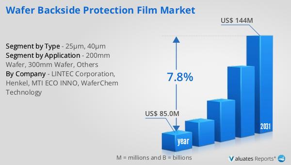
The outlook for the Global Wafer Backside Protection Film Market indicates a promising future, with significant growth expected over the coming years. In 2024, the market was valued at approximately US$ 85.0 million, reflecting the increasing demand for semiconductor components across various industries. This demand is driven by the rapid advancement of technology and the growing integration of electronic devices in everyday life. As a result, the need for reliable and effective wafer backside protection films is on the rise. By 2031, the market is projected to reach a revised size of US$ 144 million, growing at a compound annual growth rate (CAGR) of 7.8% during the forecast period. This growth is indicative of the critical role that wafer backside protection films play in the semiconductor manufacturing process, providing essential protection to the delicate wafer surfaces and ensuring the quality and performance of the final semiconductor products. The market's expansion is also supported by continuous innovation in film technology, with manufacturers striving to develop films that offer better protection, are easier to apply, and can withstand the rigorous conditions of semiconductor fabrication. As the semiconductor industry continues to grow and evolve, the Global Wafer Backside Protection Film Market is poised to play a vital role in supporting this growth, ensuring that semiconductor components remain reliable and efficient.
| Report Metric | Details |
| Report Name | Wafer Backside Protection Film Market |
| Accounted market size in year | US$ 85.0 million |
| Forecasted market size in 2031 | US$ 144 million |
| CAGR | 7.8% |
| Base Year | year |
| Forecasted years | 2025 - 2031 |
| Segment by Type |
|
| Segment by Application |
|
| Production by Region |
|
| Consumption by Region |
|
| By Company | LINTEC Corporation, Henkel, MTI ECO INNO, WaferChem Technology |
| Forecast units | USD million in value |
| Report coverage | Revenue and volume forecast, company share, competitive landscape, growth factors and trends |