What is Global Wafer Backside Grinding Service Market?
The Global Wafer Backside Grinding Service Market is a specialized segment within the semiconductor industry that focuses on the thinning of silicon wafers. These wafers are essential components in the manufacturing of integrated circuits and other semiconductor devices. The backside grinding process involves removing material from the back of the wafer to achieve a desired thickness, which is crucial for enhancing the performance and reliability of semiconductor devices. This service is vital for producing thinner, lighter, and more efficient electronic components, which are in high demand across various industries. The market for wafer backside grinding services is driven by the increasing need for miniaturization in electronics, as well as the growing demand for high-performance devices in sectors such as consumer electronics, automotive, and telecommunications. As technology continues to advance, the importance of wafer backside grinding services is expected to grow, making it a critical component of the semiconductor manufacturing process. The market is characterized by a mix of established players and emerging companies, all striving to offer innovative solutions to meet the evolving needs of the semiconductor industry.
Conventional Grinding, Chemical Mechanical Polishing (CMP) in the Global Wafer Backside Grinding Service Market:
Conventional grinding and Chemical Mechanical Polishing (CMP) are two primary methods used in the Global Wafer Backside Grinding Service Market. Conventional grinding is a mechanical process that uses abrasive wheels to remove material from the backside of the wafer. This method is known for its efficiency and ability to achieve significant material removal rates, making it suitable for applications where speed is a priority. The process involves several steps, including coarse grinding, fine grinding, and polishing, each designed to progressively reduce the thickness of the wafer while maintaining its structural integrity. Conventional grinding is widely used due to its cost-effectiveness and ability to handle a variety of wafer sizes and materials. However, it can sometimes lead to surface damage or micro-cracks, which may affect the performance of the final semiconductor device. On the other hand, Chemical Mechanical Polishing (CMP) is a more refined process that combines chemical and mechanical forces to achieve a smooth and flat wafer surface. CMP involves the use of a slurry containing chemical agents and abrasive particles, which work together to remove material from the wafer's surface. This method is highly effective in achieving a high degree of planarity and surface smoothness, making it ideal for applications where precision is critical. CMP is often used in conjunction with conventional grinding to achieve the desired wafer thickness and surface quality. The process is particularly beneficial for advanced semiconductor devices that require stringent specifications and high-performance standards. While CMP is generally more expensive than conventional grinding, its ability to produce superior surface quality and uniformity makes it a preferred choice for high-end applications. Both conventional grinding and CMP play crucial roles in the wafer backside grinding service market, each offering unique advantages and addressing specific needs within the semiconductor manufacturing process. As the demand for smaller, more powerful electronic devices continues to grow, the importance of these processes in achieving the necessary wafer specifications cannot be overstated. Manufacturers are continually seeking ways to optimize these methods, whether through advancements in grinding wheel technology, improvements in slurry formulations, or the development of hybrid processes that combine the best features of both conventional grinding and CMP. The ongoing innovation in this field is a testament to the critical role that wafer backside grinding services play in the broader semiconductor industry, enabling the production of cutting-edge devices that power the modern world.
Consumer Electronics, Automotive Electronics, Computer and Data Center, Others in the Global Wafer Backside Grinding Service Market:
The Global Wafer Backside Grinding Service Market finds extensive usage across various sectors, including consumer electronics, automotive electronics, computer and data centers, and others. In the consumer electronics sector, the demand for thinner and more efficient devices drives the need for wafer backside grinding services. Smartphones, tablets, and wearable devices all benefit from the miniaturization enabled by this process, allowing manufacturers to pack more functionality into smaller form factors. The ability to produce thinner wafers without compromising performance is crucial for meeting consumer expectations for sleek, high-performance devices. In the automotive electronics sector, wafer backside grinding services are essential for producing the advanced semiconductor components used in modern vehicles. As cars become increasingly reliant on electronic systems for everything from engine control to infotainment, the demand for reliable and efficient semiconductor devices continues to rise. Wafer backside grinding helps ensure that these components meet the stringent size and performance requirements necessary for automotive applications, contributing to the development of safer and more efficient vehicles. The computer and data center industry also relies heavily on wafer backside grinding services to produce the high-performance chips needed for processing and storage. As data centers expand to accommodate the growing demand for cloud computing and big data analytics, the need for powerful and efficient semiconductor devices becomes more critical. Wafer backside grinding enables the production of chips that can handle the intense processing requirements of modern data centers, ensuring that they operate efficiently and reliably. Beyond these primary sectors, wafer backside grinding services are also used in a variety of other applications, including telecommunications, industrial electronics, and medical devices. In telecommunications, the demand for faster and more reliable networks drives the need for advanced semiconductor components, which benefit from the precision and efficiency of wafer backside grinding. In industrial electronics, the miniaturization of components allows for more compact and efficient systems, while in medical devices, the ability to produce small, high-performance components is crucial for developing advanced diagnostic and therapeutic equipment. Overall, the Global Wafer Backside Grinding Service Market plays a vital role in enabling the production of cutting-edge technologies across a wide range of industries, supporting the ongoing advancement of modern society.
Global Wafer Backside Grinding Service Market Outlook:
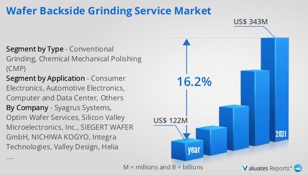
The global market for Wafer Backside Grinding Service was valued at $122 million in 2024 and is anticipated to grow significantly, reaching an estimated value of $343 million by 2031. This growth represents a compound annual growth rate (CAGR) of 16.2% over the forecast period. This impressive growth trajectory underscores the increasing importance of wafer backside grinding services in the semiconductor industry. As the demand for smaller, more efficient electronic devices continues to rise, the need for advanced wafer processing techniques becomes more critical. The market's expansion is driven by several factors, including technological advancements, the growing adoption of semiconductor devices across various industries, and the increasing focus on miniaturization and performance enhancement. The projected growth of the wafer backside grinding service market reflects the broader trends in the semiconductor industry, where innovation and efficiency are paramount. Companies operating in this market are continually investing in research and development to improve their processes and offer more advanced solutions to their customers. This includes the development of new grinding technologies, the optimization of chemical mechanical polishing techniques, and the exploration of hybrid processes that combine the strengths of both conventional grinding and CMP. As a result, the market is poised for continued growth and evolution, driven by the ever-increasing demand for high-performance semiconductor devices.
| Report Metric | Details |
| Report Name | Wafer Backside Grinding Service Market |
| Accounted market size in year | US$ 122 million |
| Forecasted market size in 2031 | US$ 343 million |
| CAGR | 16.2% |
| Base Year | year |
| Forecasted years | 2025 - 2031 |
| Segment by Type |
|
| Segment by Application |
|
| By Region |
|
| By Company | Syagrus Systems, Optim Wafer Services, Silicon Valley Microelectronics, Inc., SIEGERT WAFER GmbH, NICHIWA KOGYO, Integra Technologies, Valley Design, Helia Photonics, Aptek Industries, Enzan Factory Co., Ltd., Phoenix Silicon International, Prosperity Power Technology Inc., Huahong Group, Winstek, CHIPBOND Technology Corporation, Ceramicforum, Integrated Service Technology Inc. |
| Forecast units | USD million in value |
| Report coverage | Revenue and volume forecast, company share, competitive landscape, growth factors and trends |