What is Global Wafer AOI Machine Market?
The Global Wafer AOI Machine Market is a specialized segment within the semiconductor industry, focusing on the automated optical inspection (AOI) of wafers. Wafers are thin slices of semiconductor material, such as silicon, used in the fabrication of integrated circuits and other microdevices. AOI machines are crucial in this context as they help ensure the quality and reliability of these wafers by detecting defects and irregularities during the manufacturing process. The market for these machines is driven by the increasing demand for high-quality semiconductors, which are essential components in a wide range of electronic devices, from smartphones to advanced computing systems. As technology advances, the complexity of semiconductor devices increases, necessitating more sophisticated inspection techniques. This has led to the development of both 2D and 3D AOI technologies, which offer different capabilities in terms of defect detection and analysis. The Global Wafer AOI Machine Market is characterized by continuous innovation and competition among key players, aiming to provide more efficient and accurate inspection solutions. As the semiconductor industry continues to grow, the demand for advanced AOI machines is expected to rise, making this market a critical component of the global electronics supply chain.
Wafer 2D AOI, Wafer 3D AOI in the Global Wafer AOI Machine Market:
Wafer 2D AOI and Wafer 3D AOI are two distinct technologies used within the Global Wafer AOI Machine Market, each offering unique advantages and applications. Wafer 2D AOI primarily focuses on the surface inspection of wafers, utilizing high-resolution cameras and sophisticated image processing algorithms to detect surface defects such as scratches, contamination, and pattern deviations. This technology is highly effective for identifying defects that are visible on the wafer's surface, making it an essential tool in the early stages of semiconductor manufacturing. The simplicity and speed of 2D AOI systems make them a cost-effective solution for many manufacturers, especially when dealing with high-volume production where rapid inspection is crucial. On the other hand, Wafer 3D AOI provides a more comprehensive inspection by capturing three-dimensional data of the wafer. This technology is capable of detecting not only surface defects but also structural anomalies such as warpage, thickness variations, and other subsurface issues that might affect the performance of the final semiconductor product. 3D AOI systems use advanced sensors and imaging techniques, such as laser triangulation or structured light, to create a detailed topographical map of the wafer. This allows for a more thorough analysis and ensures that even the most subtle defects are identified and addressed. While 3D AOI systems are generally more complex and expensive than their 2D counterparts, they offer unparalleled accuracy and are indispensable in the production of high-performance semiconductors where precision is paramount. The choice between 2D and 3D AOI often depends on the specific requirements of the manufacturing process, including the type of semiconductor being produced and the acceptable defect tolerance levels. As the semiconductor industry continues to evolve, there is a growing trend towards integrating both 2D and 3D AOI technologies within a single inspection system. This hybrid approach allows manufacturers to leverage the strengths of both technologies, providing a comprehensive inspection solution that can adapt to a wide range of production scenarios. By combining the speed and efficiency of 2D AOI with the depth and precision of 3D AOI, manufacturers can achieve higher yields and better quality control, ultimately leading to more reliable and efficient semiconductor devices. The ongoing advancements in AOI technology, driven by the increasing complexity of semiconductor designs and the demand for higher quality standards, are expected to further enhance the capabilities of both 2D and 3D AOI systems. As a result, the Global Wafer AOI Machine Market is poised for significant growth, with manufacturers continually seeking innovative solutions to meet the ever-changing demands of the semiconductor industry.
AOI for IC Manufacturing, AOI for IC Packaging in the Global Wafer AOI Machine Market:
The Global Wafer AOI Machine Market plays a crucial role in two key areas of semiconductor manufacturing: AOI for IC Manufacturing and AOI for IC Packaging. In the context of IC Manufacturing, AOI machines are used to inspect wafers at various stages of the production process, ensuring that each wafer meets the stringent quality standards required for integrated circuits. During IC Manufacturing, wafers undergo multiple processes, including photolithography, etching, and doping, each of which can introduce defects. AOI machines help identify these defects early in the process, allowing manufacturers to address issues before they propagate through subsequent stages, potentially affecting the performance and yield of the final product. By providing real-time feedback and detailed defect analysis, AOI systems enable manufacturers to optimize their processes, reduce waste, and improve overall production efficiency. In the realm of IC Packaging, AOI machines are equally important. Once the integrated circuits are fabricated, they must be packaged to protect them from environmental factors and facilitate their integration into electronic devices. AOI systems are used to inspect the packaging process, ensuring that each IC is correctly encapsulated and free from defects that could compromise its functionality. This includes checking for issues such as misalignment, incomplete sealing, and contamination. The use of AOI in IC Packaging is critical for maintaining the reliability and longevity of semiconductor devices, as even minor defects in the packaging can lead to significant performance issues or failures in the field. The integration of AOI technology in both IC Manufacturing and IC Packaging underscores its importance in the semiconductor industry. By providing a comprehensive inspection solution, AOI machines help manufacturers maintain high quality standards, reduce production costs, and enhance the performance of their products. As the demand for more advanced and reliable semiconductor devices continues to grow, the role of AOI in these areas is expected to become even more significant. The ongoing development of AOI technology, including the integration of artificial intelligence and machine learning, promises to further enhance the capabilities of these systems, enabling even more precise and efficient inspections. This will be crucial in meeting the evolving demands of the semiconductor industry, where the margin for error is continually shrinking, and the need for high-quality, defect-free products is paramount.
Global Wafer AOI Machine Market Outlook:
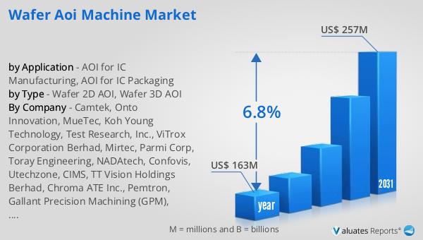
The outlook for the Global Wafer AOI Machine Market indicates a promising growth trajectory. In 2024, the market was valued at approximately US$ 163 million. Looking ahead, it is anticipated to expand significantly, reaching an estimated value of US$ 257 million by 2031. This growth is expected to occur at a compound annual growth rate (CAGR) of 6.8% over the forecast period. This upward trend reflects the increasing demand for advanced AOI machines driven by the rapid advancements in semiconductor technology and the growing need for high-quality electronic components. As the complexity of semiconductor devices continues to rise, manufacturers are investing in more sophisticated inspection solutions to ensure the reliability and performance of their products. The projected growth of the Global Wafer AOI Machine Market underscores the critical role these machines play in the semiconductor industry, providing essential quality control and defect detection capabilities. As the market evolves, manufacturers are likely to focus on developing more efficient and accurate AOI systems, incorporating cutting-edge technologies such as artificial intelligence and machine learning to enhance their inspection capabilities. This will be essential in meeting the increasing demands of the semiconductor industry and maintaining the high standards required for modern electronic devices.
| Report Metric | Details |
| Report Name | Wafer AOI Machine Market |
| Accounted market size in year | US$ 163 million |
| Forecasted market size in 2031 | US$ 257 million |
| CAGR | 6.8% |
| Base Year | year |
| Forecasted years | 2025 - 2031 |
| by Type |
|
| by Application |
|
| Production by Region |
|
| Consumption by Region |
|
| By Company | Camtek, Onto Innovation, MueTec, Koh Young Technology, Test Research, Inc., ViTrox Corporation Berhad, Mirtec, Parmi Corp, Toray Engineering, NADAtech, Confovis, Utechzone, CIMS, TT Vision Holdings Berhad, Chroma ATE Inc., Pemtron, Gallant Precision Machining (GPM), TAKAOKA TOKO, Skyverse Technology, Zhuhai Chengfeng Electronic Technology, Hangzhou Changchuan Technology, JUTZE Intelligence Technology Co., Ltd., Jiangsu VPTek Semiconductor AOI Equipment, Jiaxing Join Intelligent Equipment, The First Contact Tech Co., Ltd (TFCT), Zhongdao Optoelectronic Equipment |
| Forecast units | USD million in value |
| Report coverage | Revenue and volume forecast, company share, competitive landscape, growth factors and trends |


