What is Global Wafer Level Bump Packaging and Testing Service Market?
Global Wafer Level Bump Packaging and Testing Service Market is a specialized segment within the semiconductor industry that focuses on the packaging and testing of semiconductor wafers at the wafer level, rather than at the individual chip level.
View Full Report: https://reports.valuates.com/market-reports/QYRE-Auto-35E17913/global-wafer-level-bump-packaging-and-testing-service
Au Bump, CuNiAu Bump, Others in the Global Wafer Level Bump Packaging and Testing Service Market:
This approach involves creating tiny bumps on the surface of the wafer, which serve as connection points for the semiconductor device.
Smartphones, Wearable Devices, High-speed Data Processing, Others in the Global Wafer Level Bump Packaging and Testing Service Market:
These bumps are crucial for establishing electrical connections between the chip and the external circuitry.
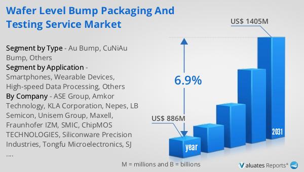
Global Wafer Level Bump Packaging and Testing Service Market Outlook:
The process of wafer level bumping is essential for the miniaturization of electronic devices, as it allows for more efficient use of space and improved performance.
Get Free Sample Report: https://reports.valuates.com/request/sample/QYRE-Auto-35E17913/global-wafer-level-bump-packaging-and-testing-service
| Report Metric | Details |
| Report Name | Wafer Level Bump Packaging and Testing Service Market |
| Accounted market size in year | US$ 886 million |
| Forecasted market size in 2031 | US$ 1405 million |
| CAGR | 6.9% |
| Base Year | year |
| Forecasted years | 2025 - 2031 |
| Segment by Type |
|
| Segment by Application |
|
| By Region |
|
| By Company | ASE Group, Amkor Technology, KLA Corporation, Nepes, LB Semicon, Unisem Group, Maxell, Fraunhofer IZM, SMIC, ChipMOS TECHNOLOGIES, Siliconware Precision Industries, Tongfu Microelectronics, SJ Semiconductor, JCET Group, Tianshui Huatian Technology, Chipmore Technology, Powertech Technology, King Yuan ELECTRONICS, Chipbond Technology, Ningbo ChipEx Semiconductor, Jiangsu Atonepoint Technology, PhySim Electronic Technology |
| Forecast units | USD million in value |
| Report coverage | Revenue and volume forecast, company share, competitive landscape, growth factors and trends |


