What is Global Semiconductor Process Chambers Market?
The Global Semiconductor Process Chambers Market is a crucial segment within the semiconductor manufacturing industry, focusing on the equipment used to create the intricate circuits found in electronic devices. These chambers are specialized environments where various processes such as etching, deposition, and implantation occur, essential for the fabrication of semiconductor wafers. The market is driven by the increasing demand for advanced electronics, including smartphones, computers, and automotive electronics, which require sophisticated semiconductor components. As technology evolves, the need for more efficient and precise semiconductor manufacturing processes grows, leading to innovations in process chamber design and functionality. The market is characterized by rapid technological advancements and a high level of competition among key players striving to enhance the efficiency and capabilities of their process chambers. This dynamic environment fosters continuous research and development, aiming to meet the ever-growing demands of the semiconductor industry. The global semiconductor process chambers market is poised for significant growth, driven by the relentless pursuit of miniaturization and performance enhancement in electronic devices, making it a vital component of the broader semiconductor manufacturing landscape.
Reaction Chamber, Transfer Chamber, Load Lock Chamber in the Global Semiconductor Process Chambers Market:
In the realm of semiconductor manufacturing, process chambers play a pivotal role, with various types such as Reaction Chambers, Transfer Chambers, and Load Lock Chambers each serving distinct functions. Reaction Chambers are integral to the chemical processes involved in semiconductor fabrication. These chambers provide a controlled environment where chemical reactions occur, crucial for processes like chemical vapor deposition (CVD) and atomic layer deposition (ALD). The precision and control offered by Reaction Chambers ensure the uniformity and quality of thin films deposited on semiconductor wafers, which is vital for the performance of the final electronic products. Transfer Chambers, on the other hand, are designed to facilitate the movement of wafers between different processing stations without exposing them to contaminants. This is essential in maintaining the integrity of the wafers, as even the slightest contamination can lead to defects in the semiconductor devices. Transfer Chambers are equipped with robotic arms and vacuum systems to ensure smooth and contamination-free wafer transfer, thereby enhancing the overall efficiency of the manufacturing process. Load Lock Chambers serve as the gateway between the external environment and the vacuum-sealed processing environment within the semiconductor fabrication equipment. These chambers allow wafers to be loaded and unloaded without compromising the vacuum conditions necessary for high-precision processes. By maintaining a vacuum seal, Load Lock Chambers prevent the introduction of contaminants and ensure that the processing environment remains stable and controlled. This is particularly important in processes that require high levels of precision and cleanliness, such as lithography and etching. The integration of these chambers into semiconductor manufacturing equipment is a testament to the complexity and precision required in the production of modern electronic devices. Each type of chamber plays a specific role in ensuring that the wafers are processed in a controlled and efficient manner, ultimately contributing to the production of high-quality semiconductor components. As the demand for more advanced and miniaturized electronic devices continues to grow, the importance of these chambers in the semiconductor manufacturing process becomes increasingly evident. The ongoing advancements in chamber technology are driven by the need to enhance the efficiency, precision, and reliability of semiconductor fabrication, making them a critical component of the global semiconductor process chambers market.
Thin Film (CVD, PVD and ALD), Etching, E-beam and Lithography, Implant, Others in the Global Semiconductor Process Chambers Market:
The Global Semiconductor Process Chambers Market finds extensive application across various areas of semiconductor manufacturing, including Thin Film processes like Chemical Vapor Deposition (CVD), Physical Vapor Deposition (PVD), and Atomic Layer Deposition (ALD), as well as Etching, E-beam and Lithography, Implant, and other specialized processes. In Thin Film processes, semiconductor process chambers are essential for depositing uniform layers of materials onto wafers. CVD and ALD processes rely on Reaction Chambers to facilitate chemical reactions that result in the deposition of thin films with precise thickness and composition. PVD, on the other hand, involves the physical transfer of material from a source to the wafer surface, requiring chambers that can maintain high vacuum conditions to ensure the purity and quality of the deposited films. These processes are critical for creating the various layers that make up semiconductor devices, influencing their electrical properties and performance. Etching processes utilize semiconductor process chambers to selectively remove material from the wafer surface, creating the intricate patterns necessary for circuit formation. The precision and control offered by these chambers are crucial in achieving the desired etch profiles and ensuring the integrity of the underlying layers. E-beam and Lithography processes also rely on specialized chambers to create the fine patterns required for semiconductor devices. These processes involve the use of electron beams or light to transfer patterns onto the wafer surface, necessitating chambers that can provide the necessary environmental conditions for accurate patterning. Implant processes involve the introduction of dopants into the semiconductor material to modify its electrical properties. Process chambers used in implantation must provide precise control over the energy and dose of the implanted ions to achieve the desired electrical characteristics. Other specialized processes in semiconductor manufacturing, such as annealing and cleaning, also rely on process chambers to provide the necessary environmental conditions for optimal results. The versatility and precision of semiconductor process chambers make them indispensable in the production of modern electronic devices, enabling the fabrication of complex and high-performance semiconductor components. As the demand for more advanced and miniaturized electronic devices continues to grow, the role of process chambers in semiconductor manufacturing becomes increasingly critical, driving ongoing advancements in chamber technology and contributing to the growth of the global semiconductor process chambers market.
Global Semiconductor Process Chambers Market Outlook:
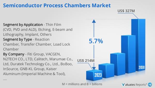
The global market for Semiconductor Process Chambers was valued at $247 million in 2024 and is anticipated to expand to a revised size of $361 million by 2031, reflecting a compound annual growth rate (CAGR) of 5.7% during the forecast period. According to SEMI, worldwide sales of semiconductor manufacturing equipment saw a 5% increase, rising from $102.6 billion in 2021 to an unprecedented $107.6 billion in 2022. For the third consecutive year, China maintained its position as the largest semiconductor equipment market in 2022, despite experiencing a 5% slowdown in investment growth year over year, accounting for $28.3 billion in billings. This growth trajectory underscores the increasing demand for semiconductor process chambers, driven by the relentless pursuit of technological advancements and the need for more efficient and precise semiconductor manufacturing processes. The market's expansion is fueled by the continuous evolution of electronic devices, which require sophisticated semiconductor components to meet the demands of modern technology. As the semiconductor industry continues to innovate and push the boundaries of what is possible, the role of process chambers in enabling these advancements becomes increasingly vital, solidifying their position as a critical component of the semiconductor manufacturing landscape.
| Report Metric | Details |
| Report Name | Semiconductor Process Chambers Market |
| Accounted market size in year | US$ 247 million |
| Forecasted market size in 2031 | US$ 361 million |
| CAGR | 5.7% |
| Base Year | year |
| Forecasted years | 2025 - 2031 |
| by Type |
|
| by Application |
|
| Production by Region |
|
| Consumption by Region |
|
| By Company | Fiti Group, VACGEN, N2TECH CO., LTD, Calitech, Marumae Co., Ltd, Duratek Technology Co., Ltd., BoBoo, InSource, GNB-KL Group, Kaiser Aluminum (Imperial Machine & Tool), LACO Technologies, Sprint Precision Technologies Co., Ltd, KFMI, Shenyang Fortune Precision Equipment Co., Ltd, Tolerance Technology (Shanghai), Sanyue Semiconductor Technology |
| Forecast units | USD million in value |
| Report coverage | Revenue and volume forecast, company share, competitive landscape, growth factors and trends |


