What is Global Semiconductor Package Inspection Probes Market?
The Global Semiconductor Package Inspection Probes Market is a crucial segment within the semiconductor industry, focusing on the tools and technologies used to inspect semiconductor packages. These probes are essential for ensuring the quality and reliability of semiconductor devices, which are integral to a wide range of electronic products. As the demand for advanced electronics continues to grow, so does the need for precise and efficient inspection methods. Semiconductor package inspection probes are designed to test and verify the integrity of semiconductor packages, ensuring they meet the required specifications and standards. This market encompasses various types of probes, each tailored to specific inspection needs and applications. The growth of this market is driven by the increasing complexity of semiconductor devices, the need for higher performance standards, and the rapid advancements in technology. As a result, manufacturers and researchers are continually developing new and improved probes to meet the evolving demands of the industry. The Global Semiconductor Package Inspection Probes Market is expected to expand significantly in the coming years, driven by technological advancements and the increasing demand for high-quality semiconductor devices.
Elastic Probes, Cantilever Probes, Vertical Probes, Others in the Global Semiconductor Package Inspection Probes Market:
Elastic probes, cantilever probes, vertical probes, and other types of probes play a vital role in the Global Semiconductor Package Inspection Probes Market. Elastic probes are designed to provide flexibility and adaptability during the inspection process. They are typically made from materials that allow them to bend and stretch without breaking, making them ideal for inspecting delicate or irregularly shaped semiconductor packages. These probes are often used in applications where precision and accuracy are paramount, as they can conform to the shape of the package being inspected, ensuring a thorough examination. Cantilever probes, on the other hand, are characterized by their rigid structure and are often used in applications where stability and durability are required. These probes are typically mounted on a fixed base and extend outwards, allowing them to reach into tight spaces and inspect hard-to-reach areas of a semiconductor package. Cantilever probes are known for their high precision and are often used in applications where minute details need to be inspected. Vertical probes are another type of probe used in the semiconductor package inspection process. These probes are designed to move vertically, allowing them to inspect the top and bottom surfaces of a semiconductor package. Vertical probes are often used in applications where a comprehensive inspection of the entire package is required, as they can easily move between different layers and surfaces. Other types of probes used in the Global Semiconductor Package Inspection Probes Market include specialized probes designed for specific applications or types of semiconductor packages. These probes may be designed to inspect specific features or characteristics of a package, such as its electrical properties or thermal performance. As the semiconductor industry continues to evolve, the demand for specialized probes is expected to grow, driving further innovation and development in this market. Each type of probe offers unique advantages and is suited to different inspection needs, making them an essential component of the semiconductor package inspection process.
Chip Design Factory, IDM Enterprises, Wafer Foundry, Packaging and Testing Plant, Others in the Global Semiconductor Package Inspection Probes Market:
The Global Semiconductor Package Inspection Probes Market finds its application in various areas, including chip design factories, IDM enterprises, wafer foundries, packaging and testing plants, and others. In chip design factories, inspection probes are used to ensure that the semiconductor packages meet the design specifications and performance standards. These probes help identify any defects or inconsistencies in the packages, allowing designers to make necessary adjustments before mass production. This ensures that the final product is of high quality and meets the required performance standards. IDM enterprises, which are integrated device manufacturers, also rely heavily on semiconductor package inspection probes. These enterprises are involved in the entire semiconductor manufacturing process, from design to production. Inspection probes are used at various stages of the manufacturing process to ensure that the packages meet the required specifications and standards. This helps IDM enterprises maintain high-quality standards and ensure the reliability of their products. Wafer foundries, which specialize in the production of semiconductor wafers, also use inspection probes to ensure the quality of their products. These probes are used to inspect the wafers for any defects or inconsistencies, ensuring that they meet the required specifications before being used in the production of semiconductor packages. Packaging and testing plants, which are responsible for the final assembly and testing of semiconductor packages, also rely on inspection probes to ensure the quality and reliability of their products. These probes are used to test the electrical and thermal performance of the packages, ensuring that they meet the required standards before being shipped to customers. Other areas where semiconductor package inspection probes are used include research and development facilities, where they are used to test new designs and technologies, and quality control departments, where they are used to ensure that the final products meet the required standards. Overall, the Global Semiconductor Package Inspection Probes Market plays a crucial role in ensuring the quality and reliability of semiconductor devices, making it an essential component of the semiconductor industry.
Global Semiconductor Package Inspection Probes Market Outlook:
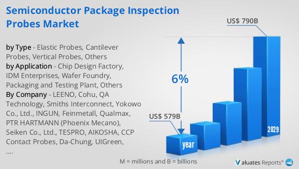
The global semiconductor market was valued at approximately $579 billion in 2022, and it is anticipated to reach around $790 billion by 2029, reflecting a compound annual growth rate (CAGR) of 6% over the forecast period. This growth is indicative of the increasing demand for semiconductor devices across various industries, driven by technological advancements and the proliferation of electronic devices. The semiconductor industry is a cornerstone of modern technology, providing the essential components that power a wide range of electronic products, from smartphones and computers to automotive systems and industrial machinery. As the world becomes increasingly digital, the demand for semiconductors is expected to continue its upward trajectory. The projected growth of the semiconductor market underscores the importance of innovation and efficiency in the production and inspection of semiconductor devices. As the market expands, so too does the need for advanced inspection technologies, such as semiconductor package inspection probes, to ensure the quality and reliability of these critical components. The growth of the semiconductor market presents significant opportunities for manufacturers, researchers, and investors, as they work to meet the evolving demands of the industry and capitalize on the increasing demand for high-quality semiconductor devices.
| Report Metric | Details |
| Report Name | Semiconductor Package Inspection Probes Market |
| Accounted market size in year | US$ 579 billion |
| Forecasted market size in 2029 | US$ 790 billion |
| CAGR | 6% |
| Base Year | year |
| Forecasted years | 2025 - 2029 |
| by Type |
|
| by Application |
|
| Production by Region |
|
| Consumption by Region |
|
| By Company | LEENO, Cohu, QA Technology, Smiths Interconnect, Yokowo Co., Ltd., INGUN, Feinmetall, Qualmax, PTR HARTMANN (Phoenix Mecano), Seiken Co., Ltd., TESPRO, AIKOSHA, CCP Contact Probes, Da-Chung, UIGreen, Centalic, Woodking Tech, Lanyi Electronic, Merryprobe Electronic, Tough Tech, Hua Rong |
| Forecast units | USD million in value |
| Report coverage | Revenue and volume forecast, company share, competitive landscape, growth factors and trends |


