What is Global EUV Lithography Service Market?
The Global EUV Lithography Service Market is a specialized segment within the semiconductor manufacturing industry that focuses on the use of extreme ultraviolet (EUV) lithography technology. EUV lithography is a cutting-edge process used to create extremely small and precise patterns on semiconductor wafers, which are essential for producing advanced microchips. This technology utilizes light with a very short wavelength, allowing for the production of smaller and more densely packed transistors on a chip. As the demand for more powerful and efficient electronic devices continues to grow, the need for advanced lithography techniques like EUV becomes increasingly important. The market for EUV lithography services encompasses various components and services, including the development and maintenance of EUV equipment, the provision of technical support, and the supply of necessary materials. Companies operating in this market are typically involved in the research, development, and commercialization of EUV technology, working closely with semiconductor manufacturers to enhance chip performance and production efficiency. The growth of this market is driven by the ongoing advancements in semiconductor technology and the increasing complexity of integrated circuits, which require more sophisticated manufacturing processes.
Light Source, Exposure Device, EUV Pod, Others in the Global EUV Lithography Service Market:
In the Global EUV Lithography Service Market, several key components play crucial roles in the overall process, including the light source, exposure device, EUV pod, and other supporting technologies. The light source is a fundamental element in EUV lithography, as it generates the extreme ultraviolet light necessary for the lithography process. This light is produced by exciting a plasma, typically using a laser, to emit EUV radiation. The efficiency and stability of the light source are critical for achieving high-resolution patterning on semiconductor wafers. The exposure device, also known as the scanner, is responsible for projecting the EUV light onto the wafer through a series of optical elements. This device must be precisely calibrated to ensure accurate pattern transfer, and it often incorporates advanced optics and control systems to manage the delicate EUV light. The EUV pod is a specialized container used to transport and store the photomask, which contains the pattern to be transferred onto the wafer. The pod is designed to protect the photomask from contamination and damage, ensuring that the pattern remains intact throughout the lithography process. Other supporting technologies in the EUV lithography service market include metrology tools, which are used to measure and verify the accuracy of the patterns created on the wafers, and cleaning systems, which help maintain the cleanliness of the equipment and materials used in the process. These components work together to enable the precise and efficient production of advanced semiconductor devices, meeting the growing demands of the electronics industry.
Integrated Device Manufacturers (IDM), Foundry, Others in the Global EUV Lithography Service Market:
The Global EUV Lithography Service Market finds significant application in various areas, including Integrated Device Manufacturers (IDM), foundries, and other sectors within the semiconductor industry. Integrated Device Manufacturers are companies that design, manufacture, and sell their own semiconductor products. For IDMs, EUV lithography is a critical technology that enables them to produce highly advanced and competitive microchips. By utilizing EUV lithography, IDMs can achieve smaller feature sizes and higher transistor densities on their chips, leading to improved performance and energy efficiency. This capability is essential for developing cutting-edge products such as high-performance processors, memory chips, and system-on-chip (SoC) solutions. Foundries, on the other hand, are companies that specialize in manufacturing semiconductor devices for other companies. They provide fabrication services to fabless semiconductor companies, which design chips but do not have their own manufacturing facilities. For foundries, offering EUV lithography services is a key differentiator that allows them to attract and retain customers seeking advanced manufacturing capabilities. By incorporating EUV technology into their production processes, foundries can offer their clients the ability to produce next-generation chips with enhanced performance and reduced power consumption. Other sectors within the semiconductor industry, such as research institutions and equipment suppliers, also benefit from the advancements in EUV lithography. Research institutions use EUV technology to explore new materials and processes for semiconductor manufacturing, while equipment suppliers develop and provide the necessary tools and components for EUV lithography systems. Overall, the Global EUV Lithography Service Market plays a vital role in enabling the semiconductor industry to meet the increasing demands for more powerful and efficient electronic devices.
Global EUV Lithography Service Market Outlook:
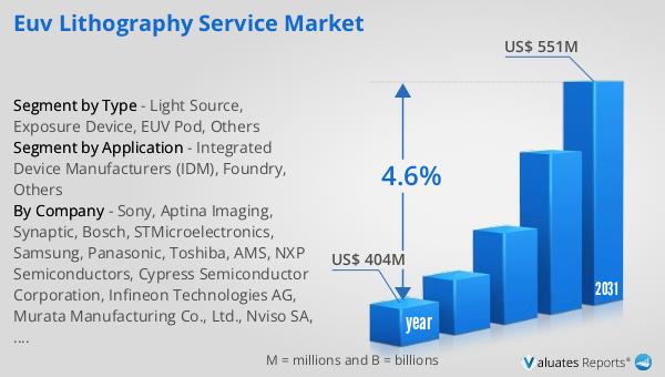
The outlook for the Global EUV Lithography Service Market indicates a promising growth trajectory over the coming years. In 2024, the market was valued at approximately US$ 404 million, reflecting the increasing adoption of EUV technology in semiconductor manufacturing. This growth is driven by the continuous advancements in semiconductor technology and the rising demand for more powerful and efficient electronic devices. By 2031, the market is projected to reach a revised size of US$ 551 million, representing a compound annual growth rate (CAGR) of 4.6% during the forecast period. This steady growth underscores the importance of EUV lithography in enabling the production of advanced microchips with smaller feature sizes and higher transistor densities. As semiconductor manufacturers strive to meet the demands of emerging technologies such as artificial intelligence, 5G, and the Internet of Things (IoT), the need for EUV lithography services is expected to increase. Companies operating in this market are likely to invest in research and development to enhance the capabilities of EUV technology and improve the efficiency of their manufacturing processes. The Global EUV Lithography Service Market is poised to play a crucial role in shaping the future of the semiconductor industry, driving innovation and enabling the development of next-generation electronic devices.
| Report Metric | Details |
| Report Name | EUV Lithography Service Market |
| Accounted market size in year | US$ 404 million |
| Forecasted market size in 2031 | US$ 551 million |
| CAGR | 4.6% |
| Base Year | year |
| Forecasted years | 2025 - 2031 |
| Segment by Type |
|
| Segment by Application |
|
| By Region |
|
| By Company | Sony, Aptina Imaging, Synaptic, Bosch, STMicroelectronics, Samsung, Panasonic, Toshiba, AMS, NXP Semiconductors, Cypress Semiconductor Corporation, Infineon Technologies AG, Murata Manufacturing Co., Ltd., Nviso SA, Omron Corporation, TE Connectivity Ltd. |
| Forecast units | USD million in value |
| Report coverage | Revenue and volume forecast, company share, competitive landscape, growth factors and trends |


