What is Global NOR Flash Chip Packaging and Testing Service Market?
The Global NOR Flash Chip Packaging and Testing Service Market is a specialized segment within the semiconductor industry that focuses on the packaging and testing of NOR flash memory chips. NOR flash memory is a type of non-volatile storage technology that retains data even when the power is turned off, making it essential for a wide range of electronic devices. The packaging process involves enclosing the delicate semiconductor material in a protective casing to ensure durability and reliability during use. Testing services are crucial to verify the functionality and performance of these chips before they are integrated into consumer products. This market is driven by the increasing demand for reliable and efficient memory solutions in various applications, including consumer electronics, automotive, and industrial sectors. As technology advances, the need for sophisticated packaging and testing services grows, ensuring that NOR flash chips meet the high standards required by modern devices. The market is characterized by continuous innovation and development to keep pace with the evolving needs of the electronics industry, making it a dynamic and essential component of the global semiconductor landscape.
Chip Probe, Final Test in the Global NOR Flash Chip Packaging and Testing Service Market:
Chip Probe and Final Test are critical stages in the Global NOR Flash Chip Packaging and Testing Service Market, ensuring that each chip meets the necessary quality and performance standards before reaching the consumer. The Chip Probe process involves testing the semiconductor wafers at the die level before they are cut and packaged. This step is crucial as it identifies any defects or issues early in the production process, allowing manufacturers to address them before incurring the additional costs of packaging. During the Chip Probe stage, each die on the wafer is tested for electrical functionality, ensuring that it meets the required specifications. This process involves using specialized equipment to make contact with the tiny pads on each die, applying test signals, and measuring the responses. The data collected during this stage helps manufacturers determine the yield of functional chips from each wafer, which is a critical factor in the overall cost and efficiency of production. Once the chips pass the Chip Probe stage, they move on to the packaging process, where they are enclosed in protective casings. After packaging, the chips undergo the Final Test, which is the last quality control step before they are shipped to customers. The Final Test involves subjecting the packaged chips to a series of rigorous tests to ensure they function correctly under various conditions. This includes testing for electrical performance, thermal stability, and reliability. The Final Test is essential for verifying that the chips can withstand the demands of real-world applications and meet the high standards required by the industry. Any chips that fail the Final Test are rejected, ensuring that only the highest quality products reach the market. The combination of Chip Probe and Final Test processes ensures that NOR flash chips are reliable, efficient, and ready for integration into a wide range of electronic devices. These testing stages are vital for maintaining the reputation and competitiveness of manufacturers in the Global NOR Flash Chip Packaging and Testing Service Market. As technology continues to evolve, the importance of these testing processes will only increase, driving further innovation and development in the industry.
Smart Wearable Device, Consumer Electronics, Internet Equipment, Others in the Global NOR Flash Chip Packaging and Testing Service Market:
The Global NOR Flash Chip Packaging and Testing Service Market plays a crucial role in several key areas, including smart wearable devices, consumer electronics, internet equipment, and other applications. In smart wearable devices, NOR flash memory is essential for storing firmware, user data, and application code. These devices, such as smartwatches and fitness trackers, require reliable and efficient memory solutions to function effectively. The packaging and testing services ensure that the NOR flash chips used in these devices are durable and capable of withstanding the various environmental conditions they may encounter during use. In consumer electronics, NOR flash memory is widely used in products like digital cameras, MP3 players, and gaming consoles. These devices rely on NOR flash for fast read speeds and reliable data storage, making the quality and performance of the chips critical to the overall user experience. The packaging and testing services help ensure that the NOR flash chips meet the high standards required by these consumer products, providing users with a seamless and enjoyable experience. In internet equipment, such as routers and modems, NOR flash memory is used to store firmware and configuration data. The reliability and stability of these chips are crucial for maintaining network performance and security. The packaging and testing services play a vital role in ensuring that the NOR flash chips used in internet equipment are robust and capable of handling the demands of continuous operation. In addition to these specific applications, the Global NOR Flash Chip Packaging and Testing Service Market also serves a wide range of other industries, including automotive, industrial, and telecommunications. In the automotive sector, NOR flash memory is used in various electronic control units (ECUs) for functions such as engine management and infotainment systems. The packaging and testing services ensure that the NOR flash chips used in these applications are reliable and capable of withstanding the harsh conditions often encountered in automotive environments. In industrial applications, NOR flash memory is used in equipment such as programmable logic controllers (PLCs) and human-machine interfaces (HMIs). The packaging and testing services help ensure that the NOR flash chips used in these applications are durable and capable of withstanding the demanding conditions often encountered in industrial settings. Overall, the Global NOR Flash Chip Packaging and Testing Service Market is essential for ensuring the quality and reliability of NOR flash memory in a wide range of applications, helping to drive innovation and development across multiple industries.
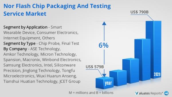
Global NOR Flash Chip Packaging and Testing Service Market Outlook:
The semiconductor industry is a rapidly evolving field, and the global market for semiconductors was valued at approximately $579 billion in 2022. This market is projected to grow significantly, reaching an estimated $790 billion by 2029. This growth represents a compound annual growth rate (CAGR) of 6% over the forecast period. This expansion is driven by the increasing demand for advanced electronic devices and the continuous development of new technologies. As the world becomes more interconnected and reliant on digital solutions, the need for efficient and reliable semiconductor components continues to rise. This growth is not only a reflection of the increasing demand for consumer electronics but also the expanding applications of semiconductors in various industries, including automotive, healthcare, and telecommunications. The semiconductor market's growth is further fueled by the ongoing advancements in technology, such as the development of artificial intelligence, the Internet of Things (IoT), and 5G networks. These innovations require sophisticated semiconductor solutions to function effectively, driving the demand for high-quality components. As a result, the semiconductor industry is poised for continued growth and development, with the Global NOR Flash Chip Packaging and Testing Service Market playing a crucial role in ensuring the quality and reliability of these essential components.
| Report Metric | Details |
| Report Name | NOR Flash Chip Packaging and Testing Service Market |
| Accounted market size in year | US$ 579 billion |
| Forecasted market size in 2029 | US$ 790 billion |
| CAGR | 6% |
| Base Year | year |
| Forecasted years | 2024 - 2029 |
| Segment by Type |
|
| Segment by Application |
|
| By Region |
|
| By Company | ASE Technology, Amkor Technology, Micron Technology, Spansion, Macronix, Winbond Electronics, Samsung Electronics, Intel, Siliconware Precision, Jinglong Technology, Tongfu Microelectronics, Wuxi Huarun Anseng, Tianshui Huatian Technology, JCET Group |
| Forecast units | USD million in value |
| Report coverage | Revenue and volume forecast, company share, competitive landscape, growth factors and trends |


