Saturday, September 28, 2024

Global PCB Processing Equipment Market Research Report 2024

What is Global PCB Processing Equipment Market?

The Global PCB Processing Equipment Market refers to the worldwide industry involved in the manufacturing and distribution of equipment used to produce printed circuit boards (PCBs). PCBs are essential components in virtually all electronic devices, providing the physical platform for mounting and interconnecting electronic components. The market encompasses a wide range of machinery and tools designed to handle various stages of PCB production, from initial design and prototyping to mass production and quality control. This includes equipment for drilling, etching, plating, and testing PCBs, among other processes. The demand for PCB processing equipment is driven by the growing electronics industry, advancements in technology, and the increasing complexity of electronic devices. As electronic devices become more sophisticated and miniaturized, the need for high-precision and efficient PCB processing equipment continues to rise. This market is crucial for ensuring the production of reliable and high-quality PCBs, which are fundamental to the functionality of modern electronic products.
PCB Processing Equipment Market

PCB Exposure Equipment, AOI/AVI Equipment, Stripping Equipment, Etching Equipment, Developing Equipment, PCB Drilling Machine, PCB Depaneling Routers, Pretreatment Process Equipment, VCP Equipment, PTH, Flying Probe Tester and Others in the Global PCB Processing Equipment Market:

PCB Exposure Equipment is used in the photolithography process to transfer circuit patterns onto the PCB substrate. This equipment uses light to expose a photoresist-coated PCB to a patterned mask, creating the desired circuit layout. AOI (Automated Optical Inspection) and AVI (Automated Visual Inspection) Equipment are essential for quality control, as they automatically inspect PCBs for defects such as misalignments, short circuits, and open circuits. Stripping Equipment is used to remove unwanted materials from the PCB surface, such as photoresist or other coatings, ensuring a clean and precise circuit pattern. Etching Equipment is crucial for removing excess copper from the PCB, leaving behind the desired circuit traces. Developing Equipment is used to develop the exposed photoresist, revealing the circuit pattern on the PCB. PCB Drilling Machines are used to create precise holes in the PCB for component mounting and interconnections. PCB Depaneling Routers are used to separate individual PCBs from a larger panel, ensuring clean and accurate cuts. Pretreatment Process Equipment prepares the PCB surface for subsequent processing steps, such as cleaning and roughening. VCP (Vertical Continuous Plating) Equipment is used for electroplating the PCB, providing a conductive layer for electrical connections. PTH (Plated Through Hole) Equipment is used to create plated through-holes, which are essential for connecting different layers of the PCB. Flying Probe Testers are used for electrical testing of PCBs, ensuring that all connections are functioning correctly. Other equipment in the PCB processing market includes various tools and machines for specific tasks, such as soldering, laminating, and cutting. Each piece of equipment plays a vital role in the PCB manufacturing process, contributing to the production of high-quality and reliable PCBs.

IC Substrate, Flexible PCBs, HDI Board, Multilayer PCBs in the Global PCB Processing Equipment Market:

The Global PCB Processing Equipment Market finds extensive usage in various types of PCBs, including IC Substrates, Flexible PCBs, HDI Boards, and Multilayer PCBs. IC Substrates are specialized PCBs used as the base for integrated circuits (ICs), providing a platform for mounting and interconnecting ICs with other components. The precision and reliability of PCB processing equipment are crucial for producing high-quality IC substrates, which are essential for the performance of ICs. Flexible PCBs are designed to be bent and folded, making them ideal for applications where space is limited or where the PCB needs to conform to a specific shape. PCB processing equipment used for flexible PCBs must be capable of handling the unique properties of flexible materials, ensuring accurate and reliable production. HDI (High-Density Interconnect) Boards are advanced PCBs with a higher density of interconnections, allowing for more complex and compact designs. The production of HDI boards requires high-precision equipment to achieve the necessary level of detail and accuracy. Multilayer PCBs consist of multiple layers of circuitry stacked together, providing increased functionality and performance. The manufacturing of multilayer PCBs involves complex processes, including lamination, drilling, and plating, all of which require specialized equipment to ensure quality and reliability. The Global PCB Processing Equipment Market plays a critical role in the production of these various types of PCBs, enabling the development of advanced electronic devices with enhanced performance and functionality.

Global PCB Processing Equipment Market Outlook:

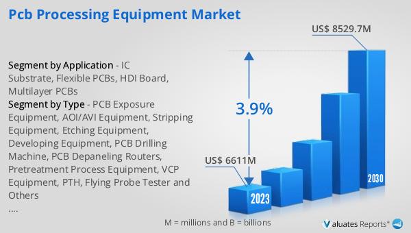
The global PCB Processing Equipment market was valued at US$ 6611 million in 2023 and is anticipated to reach US$ 8529.7 million by 2030, witnessing a CAGR of 3.9% during the forecast period 2024-2030. This market growth reflects the increasing demand for advanced PCB processing equipment driven by the rapid advancements in electronic devices and technology. As electronic devices become more complex and miniaturized, the need for high-precision and efficient PCB processing equipment continues to rise. The market encompasses a wide range of machinery and tools designed to handle various stages of PCB production, from initial design and prototyping to mass production and quality control. This includes equipment for drilling, etching, plating, and testing PCBs, among other processes. The demand for PCB processing equipment is driven by the growing electronics industry, advancements in technology, and the increasing complexity of electronic devices. This market is crucial for ensuring the production of reliable and high-quality PCBs, which are fundamental to the functionality of modern electronic products.


Report Metric Details
Report Name PCB Processing Equipment Market
Accounted market size in 2023 US$ 6611 million
Forecasted market size in 2030 US$ 8529.7 million
CAGR 3.9%
Base Year 2023
Forecasted years 2024 - 2030
Segment by Type
  • PCB Exposure Equipment
  • AOI/AVI Equipment
  • Stripping Equipment
  • Etching Equipment
  • Developing Equipment
  • PCB Drilling Machine
  • PCB Depaneling Routers
  • Pretreatment Process Equipment
  • VCP Equipment
  • PTH, Flying Probe Tester and Others
Segment by Application
  • IC Substrate
  • Flexible PCBs
  • HDI Board
  • Multilayer PCBs
By Region
  • North America (United States, Canada)
  • Europe (Germany, France, UK, Italy, Russia) Rest of Europe
  • Nordic Countries
  • Asia-Pacific (China, Japan, South Korea)
  • Southeast Asia (India, Australia)
  • Rest of Asia
  • Latin America (Mexico, Brazil)
  • Rest of Latin America
  • Middle East & Africa (Turkey, Saudi Arabia, UAE, Rest of MEA)
By Company Ninomiya System CO., Ltd., Screen, Ishii Hyoki, Centrotherm, Hakuto.co.ltd, TONETS Corp., Notion Systems GmbH, Via Mechanics, Ltd., Orbotech (KLA), ADTEC, Chime Ball Technology, ORC Manufacturing, Manz (KLEO), Ofuna Technology Co., Ltd., Symtek Automation, C SUN, AMPOC, GROUP UP Industrial (GP), Gallant Precision Machining (GPM), Eclat Forever Company, Utechzone, Ta Liang Technology, MACHVISION Inc Co., LTD, GigaVis, CIMS, Favite, FUSEI MENIX, Trumpf, Mycronic (atg), INSPEC, Saki Corporation, Omron, Koh Young, Test Research, Inc(TRI), Viscom, Mek (Marantz Electronics), Nordson, ViTrox, CyberOptics, Machine Vision Products, CKD Corporation, SCHMID, Genitec, ASYS Group, MSTECH, Atotech (MKS), Advanced Engineering (AE), Amada, LPKF, Mitsubishi Electric, EO Technics, Trotec
Forecast units USD million in value
Report coverage Revenue and volume forecast, company share, competitive landscape, growth factors and trends

Global Photomask Processing Equipment Market Research Report 2024

What is Global Photomask Processing Equipment Market?

The Global Photomask Processing Equipment Market refers to the industry that manufactures and supplies equipment used in the creation and maintenance of photomasks. Photomasks are essential tools in the semiconductor and electronics industries, acting as templates for transferring circuit patterns onto semiconductor wafers. This market encompasses a variety of equipment types, including those used for direct write lithography, electron beam lithography, photomask cleaning, etching, and inspection. The demand for photomask processing equipment is driven by the continuous advancements in semiconductor technology, which require increasingly precise and complex photomasks. As technology evolves, the need for high-quality photomasks becomes more critical, pushing the market to innovate and improve the efficiency and accuracy of its equipment. The global photomask processing equipment market is a vital component of the broader semiconductor manufacturing industry, supporting the production of integrated circuits, displays, and other electronic components.

Photomask Processing Equipment Market

Direct Write Lithography (DLW), Electron Beam Lithography System (EBL), Photomask Cleaning Equipment, Photomask Etching Equipment, Photomask Inspection System in the Global Photomask Processing Equipment Market:

Direct Write Lithography (DLW) is a technique used in the photomask processing equipment market that allows for the direct writing of patterns onto a substrate without the need for a photomask. This method is highly flexible and can be used for rapid prototyping and small-scale production. Electron Beam Lithography System (EBL) is another advanced technology that uses a focused beam of electrons to create extremely fine patterns on a substrate. EBL is known for its high resolution and precision, making it ideal for creating complex and detailed photomasks. Photomask Cleaning Equipment is essential for maintaining the quality and longevity of photomasks. This equipment removes contaminants and particles that can affect the accuracy of the photomask during the lithography process. Photomask Etching Equipment is used to etch patterns onto the photomask, typically using chemical or plasma processes. This equipment must be highly precise to ensure that the patterns are accurately transferred onto the photomask. Photomask Inspection System is crucial for ensuring the quality and accuracy of photomasks. This system uses various techniques, such as optical and electron microscopy, to detect defects and ensure that the photomask meets the required specifications. Each of these equipment types plays a critical role in the photomask processing equipment market, contributing to the production of high-quality photomasks that are essential for the semiconductor and electronics industries.

Semiconductor/IC Photomask, Display/LCD Photomask, OLED/PCB Photomask, Others in the Global Photomask Processing Equipment Market:

The usage of Global Photomask Processing Equipment Market spans several key areas, including Semiconductor/IC Photomask, Display/LCD Photomask, OLED/PCB Photomask, and others. In the Semiconductor/IC Photomask area, photomask processing equipment is used to create the intricate patterns required for integrated circuits. These circuits are the building blocks of all modern electronic devices, and the precision of the photomasks directly impacts the performance and reliability of the final products. In the Display/LCD Photomask area, photomask processing equipment is used to produce the photomasks needed for liquid crystal displays (LCDs). These displays are used in a wide range of devices, from televisions and computer monitors to smartphones and tablets. The quality of the photomasks affects the clarity and resolution of the displays, making high-quality photomask processing equipment essential. In the OLED/PCB Photomask area, photomask processing equipment is used to create photomasks for organic light-emitting diode (OLED) displays and printed circuit boards (PCBs). OLED displays are known for their vibrant colors and high contrast ratios, and the precision of the photomasks is crucial for achieving these characteristics. PCBs are used in virtually all electronic devices, and the accuracy of the photomasks affects the performance and reliability of the circuits. Other areas where photomask processing equipment is used include the production of microelectromechanical systems (MEMS), sensors, and other advanced electronic components. In each of these areas, the quality and precision of the photomasks are critical for the performance and reliability of the final products, making photomask processing equipment an essential part of the manufacturing process.

Global Photomask Processing Equipment Market Outlook:

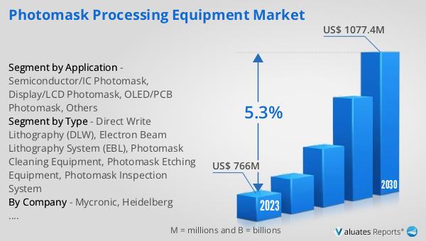
The global Photomask Processing Equipment market was valued at US$ 766 million in 2023 and is anticipated to reach US$ 1077.4 million by 2030, witnessing a CAGR of 5.3% during the forecast period 2024-2030. This growth reflects the increasing demand for high-quality photomasks driven by advancements in semiconductor and electronics technology. As the complexity and precision of electronic devices continue to evolve, the need for advanced photomask processing equipment becomes more critical. The market's growth is also supported by the continuous innovation and development of new technologies in the photomask processing equipment industry. These advancements enable manufacturers to produce more accurate and reliable photomasks, which are essential for the production of high-performance electronic components. The increasing adoption of photomask processing equipment in various applications, such as semiconductor manufacturing, display production, and PCB fabrication, further drives the market's growth. Overall, the global photomask processing equipment market is expected to experience significant growth in the coming years, driven by the ongoing advancements in technology and the increasing demand for high-quality photomasks.


Report Metric Details
Report Name Photomask Processing Equipment Market
Accounted market size in 2023 US$ 766 million
Forecasted market size in 2030 US$ 1077.4 million
CAGR 5.3%
Base Year 2023
Forecasted years 2024 - 2030
Segment by Type
  • Direct Write Lithography (DLW)
  • Electron Beam Lithography System (EBL)
  • Photomask Cleaning Equipment
  • Photomask Etching Equipment
  • Photomask Inspection System
Segment by Application
  • Semiconductor/IC Photomask
  • Display/LCD Photomask
  • OLED/PCB Photomask
  • Others
By Region
  • North America (United States, Canada)
  • Europe (Germany, France, UK, Italy, Russia) Rest of Europe
  • Nordic Countries
  • Asia-Pacific (China, Japan, South Korea)
  • Southeast Asia (India, Australia)
  • Rest of Asia
  • Latin America (Mexico, Brazil)
  • Rest of Latin America
  • Middle East & Africa (Turkey, Saudi Arabia, UAE, Rest of MEA)
By Company Mycronic, Heidelberg Instruments, JEOL, Advantest, Elionix Inc., Vistec Electron Beam GmbH, Veeco, NuFlare Technology, Inc., SÜSS MicroTec SE, Orbotech (KLA), SHIBAURA MECHATRONICS, V-Technology, ZEISS Group, Lasertec Corporation, SINTO S-PRECISION, ASML(HMI), Applied Materials, Technovision, Amaya CO., LTD, Micro Engineering Inc, Ulvac, Circuit Fabology Microelectronics Equipment Co.,Ltd., Jiangsu Yingsu IC Equipment, Beijing Hualin Jiaye
Forecast units USD million in value
Report coverage Revenue and volume forecast, company share, competitive landscape, growth factors and trends

Global Photomask Manufacturing and Inspection Equipment Market Research Report 2024

What is Global Photomask Manufacturing and Inspection Equipment Market?

The Global Photomask Manufacturing and Inspection Equipment Market is a specialized sector within the broader semiconductor and electronics industry. Photomasks are essential tools used in the photolithography process to transfer circuit patterns onto semiconductor wafers, which are then used to manufacture integrated circuits (ICs), displays, and other electronic components. The market for photomask manufacturing and inspection equipment includes various types of machinery and tools designed to create, clean, etch, and inspect these photomasks to ensure they meet the high precision and quality standards required in the industry. This market is driven by the increasing demand for advanced electronic devices, the miniaturization of semiconductor components, and the need for high-resolution displays. As technology continues to evolve, the photomask manufacturing and inspection equipment market is expected to grow, driven by innovations in semiconductor fabrication and the rising adoption of advanced manufacturing techniques.

Photomask Manufacturing and Inspection Equipment Market

Direct Write Lithography (DLW), Electron Beam Lithography System (EBL), Photomask Cleaning Equipment, Photomask Etching Equipment, Photomask Inspection System in the Global Photomask Manufacturing and Inspection Equipment Market:

Direct Write Lithography (DLW) is a technique used in the photomask manufacturing process that allows for the direct writing of patterns onto a substrate without the need for a photomask. This method is highly precise and is often used for creating complex and intricate designs that are difficult to achieve with traditional photolithography. Electron Beam Lithography System (EBL) is another advanced technique that uses a focused beam of electrons to draw custom patterns on a surface covered with an electron-sensitive film. EBL is known for its high resolution and is commonly used in research and development for creating nanoscale devices. Photomask Cleaning Equipment is essential for maintaining the quality and longevity of photomasks. These machines use various cleaning methods, such as ultrasonic cleaning, to remove contaminants and particles from the photomask surface, ensuring that the patterns are transferred accurately during the photolithography process. Photomask Etching Equipment is used to etch the desired patterns onto the photomask substrate. This equipment uses chemical or plasma etching techniques to create precise and intricate designs on the photomask, which are then used to transfer these patterns onto semiconductor wafers. Photomask Inspection Systems are critical for ensuring the quality and accuracy of photomasks. These systems use advanced imaging and analysis techniques to detect defects and irregularities in the photomask patterns, ensuring that only high-quality photomasks are used in the semiconductor manufacturing process. The combination of these advanced technologies and equipment ensures that the photomask manufacturing process is efficient, precise, and capable of meeting the high standards required in the semiconductor industry.

Semiconductor/IC Photomask, Display/LCD Photomask, OLED/PCB Photomask, Others in the Global Photomask Manufacturing and Inspection Equipment Market:

The Global Photomask Manufacturing and Inspection Equipment Market plays a crucial role in various areas, including Semiconductor/IC Photomask, Display/LCD Photomask, OLED/PCB Photomask, and others. In the semiconductor industry, photomasks are used to transfer intricate circuit patterns onto silicon wafers, which are then processed to create integrated circuits (ICs). The precision and accuracy of photomasks are critical in ensuring the performance and reliability of ICs, making photomask manufacturing and inspection equipment essential in this sector. In the display industry, photomasks are used to create patterns for LCD and OLED displays. These displays require high-resolution and high-precision photomasks to ensure the quality and clarity of the final product. Photomask manufacturing and inspection equipment are used to create and inspect these photomasks, ensuring that they meet the stringent requirements of the display industry. In the PCB (Printed Circuit Board) industry, photomasks are used to transfer circuit patterns onto the PCB substrate. The accuracy and precision of these patterns are critical in ensuring the performance and reliability of the final PCB. Photomask manufacturing and inspection equipment are used to create and inspect these photomasks, ensuring that they meet the high standards required in the PCB industry. Other areas where photomask manufacturing and inspection equipment are used include the production of MEMS (Micro-Electro-Mechanical Systems), sensors, and other advanced electronic components. The precision and accuracy of photomasks are critical in these areas, making photomask manufacturing and inspection equipment essential in ensuring the quality and performance of the final products. Overall, the Global Photomask Manufacturing and Inspection Equipment Market plays a vital role in various industries, ensuring the quality and performance of a wide range of electronic components and devices.

Global Photomask Manufacturing and Inspection Equipment Market Outlook:

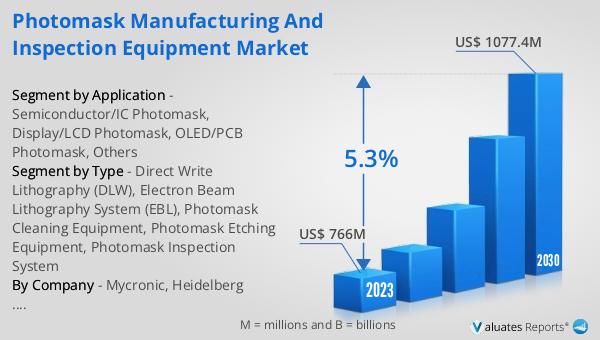
The global Photomask Manufacturing and Inspection Equipment market was valued at US$ 766 million in 2023 and is anticipated to reach US$ 1077.4 million by 2030, witnessing a CAGR of 5.3% during the forecast period 2024-2030. This growth is driven by the increasing demand for advanced electronic devices, the miniaturization of semiconductor components, and the need for high-resolution displays. As technology continues to evolve, the photomask manufacturing and inspection equipment market is expected to grow, driven by innovations in semiconductor fabrication and the rising adoption of advanced manufacturing techniques. The market outlook indicates a positive trend, with significant growth opportunities in various sectors, including semiconductor, display, and PCB industries. The increasing complexity and precision required in these industries are driving the demand for advanced photomask manufacturing and inspection equipment, ensuring the quality and performance of the final products. Overall, the market outlook for the Global Photomask Manufacturing and Inspection Equipment Market is promising, with significant growth potential in the coming years.


Report Metric Details
Report Name Photomask Manufacturing and Inspection Equipment Market
Accounted market size in 2023 US$ 766 million
Forecasted market size in 2030 US$ 1077.4 million
CAGR 5.3%
Base Year 2023
Forecasted years 2024 - 2030
Segment by Type
  • Direct Write Lithography (DLW)
  • Electron Beam Lithography System (EBL)
  • Photomask Cleaning Equipment
  • Photomask Etching Equipment
  • Photomask Inspection System
Segment by Application
  • Semiconductor/IC Photomask
  • Display/LCD Photomask
  • OLED/PCB Photomask
  • Others
By Region
  • North America (United States, Canada)
  • Europe (Germany, France, UK, Italy, Russia) Rest of Europe
  • Nordic Countries
  • Asia-Pacific (China, Japan, South Korea)
  • Southeast Asia (India, Australia)
  • Rest of Asia
  • Latin America (Mexico, Brazil)
  • Rest of Latin America
  • Middle East & Africa (Turkey, Saudi Arabia, UAE, Rest of MEA)
By Company Mycronic, Heidelberg Instruments, JEOL, Advantest, Elionix Inc., Vistec Electron Beam GmbH, Veeco, NuFlare Technology, Inc., SÜSS MicroTec SE, Orbotech (KLA), SHIBAURA MECHATRONICS, V-Technology, ZEISS Group, Lasertec Corporation, SINTO S-PRECISION, ASML(HMI), Applied Materials, Technovision, Amaya CO., LTD, Micro Engineering Inc, Ulvac, Circuit Fabology Microelectronics Equipment Co.,Ltd., Jiangsu Yingsu IC Equipment, Beijing Hualin Jiaye
Forecast units USD million in value
Report coverage Revenue and volume forecast, company share, competitive landscape, growth factors and trends

Global Photomask Lithography Equipment Market Research Report 2024

What is Global Photomask Lithography Equipment Market?

The Global Photomask Lithography Equipment Market is a specialized segment within the broader semiconductor and electronics manufacturing industry. Photomask lithography equipment is essential for the production of photomasks, which are used to transfer circuit patterns onto semiconductor wafers. These photomasks are critical in the fabrication of integrated circuits (ICs), displays, and other electronic components. The market encompasses various types of lithography equipment, including direct write lithography (DLW) and electron beam lithography (EBL) systems. These technologies enable the precise patterning required for advanced semiconductor devices and high-resolution displays. The demand for photomask lithography equipment is driven by the continuous advancements in semiconductor technology, the increasing complexity of IC designs, and the growing need for high-performance electronic devices. As the industry evolves, the market for photomask lithography equipment is expected to expand, driven by innovations in lithography techniques and the rising demand for miniaturized and efficient electronic components.

Photomask Lithography Equipment Market

Direct Write Lithography (DLW), Electron Beam Lithography System (EBL) in the Global Photomask Lithography Equipment Market:

Direct Write Lithography (DLW) and Electron Beam Lithography (EBL) are two advanced technologies within the Global Photomask Lithography Equipment Market. DLW is a maskless lithography technique that directly writes patterns onto a substrate using a focused beam of light or electrons. This method offers high flexibility and precision, making it suitable for prototyping and small-scale production. DLW is particularly advantageous for applications requiring rapid design changes and customization, as it eliminates the need for photomasks. On the other hand, Electron Beam Lithography (EBL) uses a focused beam of electrons to create extremely fine patterns on a substrate. EBL is known for its high resolution and accuracy, making it ideal for fabricating nanoscale structures and advanced semiconductor devices. EBL systems are widely used in research and development, as well as in the production of photomasks for cutting-edge semiconductor manufacturing. Both DLW and EBL play crucial roles in the photomask lithography equipment market, catering to the diverse needs of the semiconductor and electronics industries. These technologies enable the production of intricate and high-precision patterns, supporting the development of next-generation electronic devices and components. As the demand for smaller, faster, and more efficient electronic devices continues to grow, the importance of DLW and EBL in the photomask lithography equipment market is expected to increase, driving further advancements in lithography techniques and equipment.

Semiconductor/IC, Display/LCD, OLED/PCB, Others in the Global Photomask Lithography Equipment Market:

The usage of Global Photomask Lithography Equipment Market spans several key areas, including Semiconductor/IC, Display/LCD, OLED/PCB, and others. In the semiconductor industry, photomask lithography equipment is essential for the fabrication of integrated circuits (ICs). Photomasks are used to transfer intricate circuit patterns onto semiconductor wafers, enabling the production of high-performance ICs used in various electronic devices, such as smartphones, computers, and automotive electronics. The precision and accuracy of photomask lithography equipment are critical for achieving the miniaturization and complexity required in modern IC designs. In the display industry, photomask lithography equipment is used to produce high-resolution displays, including LCDs and OLEDs. Photomasks are employed to pattern the thin-film transistors (TFTs) and other components that make up the display panels. The demand for high-definition and energy-efficient displays drives the need for advanced photomask lithography equipment capable of producing fine and accurate patterns. In the PCB (Printed Circuit Board) industry, photomask lithography equipment is used to create the intricate circuitry on PCBs, which are essential for connecting and supporting electronic components in various devices. The precision of photomask lithography ensures the reliability and performance of PCBs in applications ranging from consumer electronics to industrial equipment. Additionally, photomask lithography equipment finds applications in other areas, such as MEMS (Micro-Electro-Mechanical Systems), photonics, and nanotechnology. These applications require high-precision patterning to create microscale and nanoscale structures with specific functionalities. Overall, the Global Photomask Lithography Equipment Market plays a vital role in enabling the production of advanced electronic devices and components across various industries, supporting technological innovation and development.

Global Photomask Lithography Equipment Market Outlook:

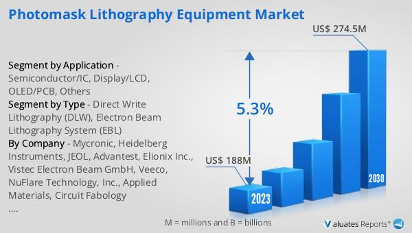
The global Photomask Lithography Equipment market was valued at US$ 188 million in 2023 and is anticipated to reach US$ 274.5 million by 2030, witnessing a CAGR of 5.3% during the forecast period 2024-2030. This growth reflects the increasing demand for advanced lithography equipment driven by the continuous advancements in semiconductor technology and the growing complexity of integrated circuit designs. The market's expansion is also fueled by the rising need for high-performance electronic devices, which require precise and accurate patterning capabilities. As the semiconductor and electronics industries continue to evolve, the demand for photomask lithography equipment is expected to grow, supporting the development of next-generation electronic components and devices. The market outlook indicates a positive trend, with significant opportunities for innovation and growth in the coming years.


Report Metric Details
Report Name Photomask Lithography Equipment Market
Accounted market size in 2023 US$ 188 million
Forecasted market size in 2030 US$ 274.5 million
CAGR 5.3%
Base Year 2023
Forecasted years 2024 - 2030
Segment by Type
  • Direct Write Lithography (DLW)
  • Electron Beam Lithography System (EBL)
Segment by Application
  • Semiconductor/IC
  • Display/LCD
  • OLED/PCB
  • Others
Production by Region
  • North America
  • Europe
  • China
  • Japan
Consumption by Region
  • North America (United States, Canada)
  • Europe (Germany, France, UK, Italy, Russia)
  • Asia-Pacific (China, Japan, South Korea, Taiwan)
  • Southeast Asia (India)
  • Latin America (Mexico, Brazil)
By Company Mycronic, Heidelberg Instruments, JEOL, Advantest, Elionix Inc., Vistec Electron Beam GmbH, Veeco, NuFlare Technology, Inc., Applied Materials, Circuit Fabology Microelectronics Equipment Co.,Ltd., Jiangsu Yingsu IC Equipment
Forecast units USD million in value
Report coverage Revenue and volume forecast, company share, competitive landscape, growth factors and trends

Global Semiconductor Photomask Writer Market Research Report 2024

What is Global Semiconductor Photomask Writer Market?

The Global Semiconductor Photomask Writer Market is a specialized segment within the semiconductor industry that focuses on the production and sale of photomask writers. Photomask writers are critical tools used in the photolithography process, which is essential for manufacturing integrated circuits (ICs) and other semiconductor devices. These writers create photomasks, which are templates that define the intricate patterns of electronic circuits on semiconductor wafers. The market for these tools is driven by the increasing demand for advanced semiconductor devices, which require highly precise and complex photomasks. As technology advances, the need for more sophisticated photomask writers grows, making this market a vital component of the semiconductor manufacturing ecosystem. The market encompasses various types of photomask writers, including laser-based and electron beam-based systems, each offering different levels of precision and speed. The growth of this market is closely tied to the overall health of the semiconductor industry, which continues to expand due to the proliferation of electronic devices and the advent of new technologies such as 5G, artificial intelligence, and the Internet of Things (IoT).

Semiconductor Photomask Writer Market

Direct Write Lithography (DLW), Electron Beam Lithography System (EBL) in the Global Semiconductor Photomask Writer Market:

Direct Write Lithography (DLW) and Electron Beam Lithography (EBL) are two advanced techniques used in the Global Semiconductor Photomask Writer Market. Direct Write Lithography (DLW) is a method that allows for the direct writing of patterns onto a substrate without the need for a photomask. This technique is highly flexible and can be used for rapid prototyping and small-scale production runs. DLW systems use focused laser beams to write patterns directly onto the photoresist-coated substrate, offering high precision and the ability to create complex geometries. This method is particularly useful for applications that require quick turnaround times and high customization, such as research and development, and the production of specialized semiconductor devices. On the other hand, Electron Beam Lithography (EBL) is a technique that uses a focused beam of electrons to write patterns onto a substrate. EBL is known for its extremely high resolution, making it ideal for creating very fine features that are beyond the capabilities of traditional photolithography. This technique is widely used in the production of advanced semiconductor devices, such as those found in cutting-edge microprocessors and memory chips. EBL systems are capable of producing patterns with feature sizes down to the nanometer scale, which is essential for the continued miniaturization of electronic components. However, EBL is generally slower and more expensive than other lithography methods, making it more suitable for applications where precision is paramount and production volumes are relatively low. Both DLW and EBL play crucial roles in the Global Semiconductor Photomask Writer Market, catering to different needs within the semiconductor manufacturing process. DLW offers flexibility and speed, making it ideal for prototyping and specialized applications, while EBL provides the high resolution needed for advanced semiconductor devices. As the demand for more sophisticated and miniaturized electronic components continues to grow, the importance of these advanced lithography techniques is expected to increase, driving further innovation and development within the photomask writer market. The integration of these technologies into the semiconductor manufacturing process helps to ensure that the industry can keep pace with the rapid advancements in electronic device technology, ultimately supporting the continued growth and evolution of the semiconductor market as a whole.

Semiconductor/IC, Display/LCD, OLED/PCB, Others in the Global Semiconductor Photomask Writer Market:

The Global Semiconductor Photomask Writer Market finds extensive usage across various sectors, including Semiconductor/IC, Display/LCD, OLED/PCB, and others. In the Semiconductor/IC sector, photomask writers are indispensable for the production of integrated circuits. These circuits are the building blocks of all electronic devices, from smartphones to supercomputers. The precision and complexity required in IC manufacturing necessitate the use of advanced photomask writers to create the intricate patterns that define the electronic circuits on semiconductor wafers. As the demand for smaller, faster, and more efficient ICs continues to grow, the role of photomask writers in this sector becomes increasingly critical. In the Display/LCD sector, photomask writers are used to produce the photomasks needed for manufacturing liquid crystal displays (LCDs). These displays are found in a wide range of devices, including televisions, computer monitors, and smartphones. The quality and resolution of LCDs are directly influenced by the precision of the photomasks used in their production. Advanced photomask writers enable manufacturers to create high-resolution displays with vibrant colors and sharp images, meeting the ever-increasing consumer demand for better display quality. The OLED/PCB sector also relies heavily on photomask writers. Organic Light Emitting Diode (OLED) displays are known for their superior color accuracy, contrast, and flexibility compared to traditional LCDs. The production of OLED displays requires highly precise photomasks to ensure the accurate deposition of organic materials onto the substrate. Similarly, in the production of Printed Circuit Boards (PCBs), photomask writers are used to create the detailed patterns that define the electrical connections between components. The growing adoption of OLED technology in various applications, from smartphones to large-screen televisions, and the increasing complexity of PCBs in modern electronic devices, drive the demand for advanced photomask writers in this sector. Beyond these primary sectors, the Global Semiconductor Photomask Writer Market also serves other areas, including the production of microelectromechanical systems (MEMS), sensors, and various types of optoelectronic devices. MEMS devices, which combine electrical and mechanical components at the microscale, are used in a wide range of applications, from automotive sensors to medical devices. The production of these devices requires highly precise photomasks to define their intricate structures. Similarly, the manufacturing of sensors and optoelectronic devices, such as photodetectors and light-emitting diodes (LEDs), relies on advanced photomask writers to achieve the necessary precision and performance. Overall, the Global Semiconductor Photomask Writer Market plays a vital role in enabling the production of a wide range of electronic devices and components. The precision and complexity required in modern electronics necessitate the use of advanced photomask writers, driving the demand for these tools across various sectors. As technology continues to advance and the demand for more sophisticated electronic devices grows, the importance of the photomask writer market is expected to increase, supporting the continued innovation and development of the semiconductor industry.

Global Semiconductor Photomask Writer Market Outlook:

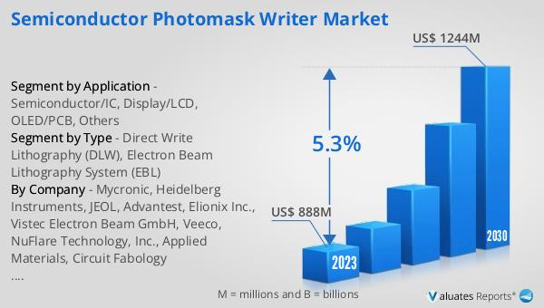
The global Semiconductor Photomask Writer market was valued at US$ 888 million in 2023 and is anticipated to reach US$ 1244 million by 2030, witnessing a CAGR of 5.3% during the forecast period 2024-2030. This market outlook highlights the significant growth potential of the photomask writer market over the coming years. The increasing demand for advanced semiconductor devices, driven by the proliferation of electronic devices and the advent of new technologies such as 5G, artificial intelligence, and the Internet of Things (IoT), is expected to fuel this growth. The market's expansion is also supported by the continuous advancements in photomask writer technology, which enable the production of more precise and complex photomasks required for modern semiconductor manufacturing. As the semiconductor industry continues to evolve and innovate, the demand for high-quality photomask writers is likely to remain strong, driving the market's growth and development.


Report Metric Details
Report Name Semiconductor Photomask Writer Market
Accounted market size in 2023 US$ 888 million
Forecasted market size in 2030 US$ 1244 million
CAGR 5.3%
Base Year 2023
Forecasted years 2024 - 2030
Segment by Type
  • Direct Write Lithography (DLW)
  • Electron Beam Lithography System (EBL)
Segment by Application
  • Semiconductor/IC
  • Display/LCD
  • OLED/PCB
  • Others
Production by Region
  • North America
  • Europe
  • China
  • Japan
Consumption by Region
  • North America (United States, Canada)
  • Europe (Germany, France, UK, Italy, Russia)
  • Asia-Pacific (China, Japan, South Korea, Taiwan)
  • Southeast Asia (India)
  • Latin America (Mexico, Brazil)
By Company Mycronic, Heidelberg Instruments, JEOL, Advantest, Elionix Inc., Vistec Electron Beam GmbH, Veeco, NuFlare Technology, Inc., Applied Materials, Circuit Fabology Microelectronics Equipment Co.,Ltd., Jiangsu Yingsu IC Equipment
Forecast units USD million in value
Report coverage Revenue and volume forecast, company share, competitive landscape, growth factors and trends

Global Ceramic Matrix Composites for Aerospace Market Research Report 2024

What is Global Ceramic Matrix Composites for Aerospace Market?

Global Ceramic Matrix Composites (CMCs) for the aerospace market are advanced materials designed to withstand extreme conditions encountered in aerospace applications. These composites are made by embedding ceramic fibers into a ceramic matrix, resulting in a material that combines the best properties of both ceramics and composites. CMCs are known for their high-temperature resistance, lightweight nature, and exceptional strength, making them ideal for aerospace components such as turbine blades, exhaust nozzles, and heat shields. The use of CMCs in aerospace helps improve fuel efficiency, reduce emissions, and enhance overall performance. As the aerospace industry continues to push the boundaries of technology, the demand for CMCs is expected to grow, driven by the need for materials that can endure the harsh environments of space and high-speed flight. The global market for CMCs in aerospace is characterized by ongoing research and development, with companies and research institutions striving to develop new formulations and manufacturing techniques to further enhance the properties and applications of these advanced materials.

Ceramic Matrix Composites for Aerospace Market

Oxide, Silicon Carbide, Carbon, Others in the Global Ceramic Matrix Composites for Aerospace Market:

Oxide, Silicon Carbide, Carbon, and other types of Ceramic Matrix Composites (CMCs) play crucial roles in the aerospace market, each offering unique properties that cater to specific applications. Oxide CMCs, typically composed of alumina or zirconia fibers embedded in an oxide matrix, are known for their excellent thermal stability and resistance to oxidation. These properties make them suitable for applications in high-temperature environments, such as turbine engines and exhaust systems, where maintaining structural integrity under extreme heat is critical. Silicon Carbide (SiC) CMCs, on the other hand, are renowned for their exceptional strength, thermal conductivity, and resistance to thermal shock. SiC CMCs are often used in components that require high mechanical performance and durability, such as turbine blades and heat exchangers. Carbon CMCs, which consist of carbon fibers in a carbon matrix, offer high strength-to-weight ratios and excellent thermal and electrical conductivity. These composites are particularly valuable in applications where weight reduction is paramount, such as in spacecraft and high-speed aircraft. Additionally, Carbon CMCs are used in brake systems and other components that require high frictional performance. Other types of CMCs, including those based on boron nitride or silicon nitride, provide specialized properties for niche applications. For instance, boron nitride CMCs offer excellent thermal and chemical stability, making them suitable for use in harsh chemical environments. Silicon nitride CMCs, known for their high fracture toughness and wear resistance, are used in applications that demand high reliability and longevity. The diversity of CMC types allows aerospace engineers to select the most appropriate material for each specific application, optimizing performance and efficiency. The development and utilization of these advanced materials are driven by the continuous pursuit of innovation in the aerospace industry, aiming to achieve higher performance, greater fuel efficiency, and reduced environmental impact. As research and development efforts continue, the range of applications for CMCs in aerospace is expected to expand, further solidifying their importance in the industry.

Commercial, Military in the Global Ceramic Matrix Composites for Aerospace Market:

The usage of Global Ceramic Matrix Composites (CMCs) in the aerospace market spans both commercial and military sectors, each with distinct requirements and applications. In the commercial aerospace sector, CMCs are primarily used to enhance the performance and efficiency of aircraft engines. The high-temperature resistance and lightweight nature of CMCs make them ideal for turbine blades, combustor liners, and exhaust nozzles, where they help improve fuel efficiency and reduce emissions. By enabling engines to operate at higher temperatures, CMCs contribute to better fuel combustion and lower specific fuel consumption, which is crucial for commercial airlines aiming to reduce operational costs and meet stringent environmental regulations. Additionally, CMCs are used in thermal protection systems and heat shields, ensuring the safety and reliability of commercial aircraft during high-speed flight and re-entry into the Earth's atmosphere. In the military aerospace sector, the use of CMCs is driven by the need for advanced materials that can withstand the extreme conditions encountered in defense applications. Military aircraft, including fighter jets and unmanned aerial vehicles (UAVs), benefit from the high strength-to-weight ratio and thermal stability of CMCs. These properties are essential for components such as engine parts, missile casings, and thermal protection systems, where performance and durability are critical. CMCs also play a vital role in enhancing the stealth capabilities of military aircraft by reducing radar cross-sections and improving thermal management. The ability of CMCs to endure high temperatures and harsh environments makes them suitable for use in hypersonic vehicles and other advanced defense systems. Furthermore, the lightweight nature of CMCs contributes to increased payload capacity and extended range for military aircraft, providing strategic advantages in defense operations. The adoption of CMCs in both commercial and military aerospace sectors is driven by the continuous pursuit of innovation and the need to meet evolving performance and environmental standards. As the aerospace industry advances, the role of CMCs is expected to grow, offering new opportunities for enhancing the capabilities and efficiency of both commercial and military aircraft.

Global Ceramic Matrix Composites for Aerospace Market Outlook:

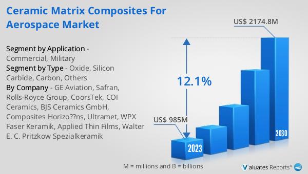
The aerospace and defense industry remains a hub of innovation, driven by the urgent need for modernization and the increasing significance of emerging technologies such as artificial intelligence and unmanned systems. In this dynamic environment, the global Ceramic Matrix Composites (CMCs) for Aerospace market has shown remarkable growth. Valued at US$ 985 million in 2023, the market is projected to reach US$ 2174.8 million by 2030, reflecting a compound annual growth rate (CAGR) of 12.1% during the forecast period from 2024 to 2030. This growth is fueled by the continuous advancements in aerospace technology and the increasing demand for materials that can withstand extreme conditions while offering superior performance. The adoption of CMCs in aerospace applications is driven by their unique properties, including high-temperature resistance, lightweight nature, and exceptional strength, which are essential for improving fuel efficiency, reducing emissions, and enhancing overall performance. As the aerospace industry continues to evolve, the role of CMCs is expected to become even more significant, contributing to the development of next-generation aircraft and defense systems.


Report Metric Details
Report Name Ceramic Matrix Composites for Aerospace Market
Accounted market size in 2023 US$ 985 million
Forecasted market size in 2030 US$ 2174.8 million
CAGR 12.1%
Base Year 2023
Forecasted years 2024 - 2030
Segment by Type
  • Oxide
  • Silicon Carbide
  • Carbon
  • Others
Segment by Application
  • Commercial
  • Military
Production by Region
  • North America
  • Europe
  • China
  • Japan
Consumption by Region
  • North America (United States, Canada)
  • Europe (Germany, France, UK, Italy, Russia)
  • Asia-Pacific (China, Japan, South Korea, Taiwan)
  • Southeast Asia (India)
  • Latin America (Mexico, Brazil)
By Company GE Aviation, Safran, Rolls-Royce Group, CoorsTek, COI Ceramics, BJS Ceramics GmbH, Composites Horizo??ns, Ultramet, WPX Faser Keramik, Applied Thin Films, Walter E. C. Pritzkow Spezialkeramik
Forecast units USD million in value
Report coverage Revenue and volume forecast, company share, competitive landscape, growth factors and trends

Global Ceramic Matrix Composites for Automobile Market Research Report 2024

What is Global Ceramic Matrix Composites for Automobile Market?

Global Ceramic Matrix Composites (CMCs) for the automobile market represent a significant advancement in automotive materials technology. These composites are engineered materials made from ceramic fibers embedded in a ceramic matrix, which combine to offer superior properties compared to traditional materials like metals and polymers. CMCs are known for their high-temperature resistance, lightweight nature, and exceptional strength, making them ideal for various automotive applications. They are particularly beneficial in enhancing fuel efficiency and reducing emissions due to their lightweight properties. Additionally, CMCs exhibit excellent wear resistance and durability, which contribute to the longevity and reliability of automotive components. The adoption of CMCs in the automobile industry is driven by the increasing demand for high-performance materials that can withstand extreme conditions while improving overall vehicle efficiency and performance. As the automotive industry continues to evolve, the role of CMCs is expected to become even more prominent, paving the way for more advanced and sustainable vehicle technologies.

Ceramic Matrix Composites for Automobile Market

Oxide, Silicon Carbide, Carbon, Others in the Global Ceramic Matrix Composites for Automobile Market:

Oxide, Silicon Carbide, Carbon, and other types of ceramic matrix composites each offer unique benefits and applications within the global ceramic matrix composites for the automobile market. Oxide CMCs, typically composed of alumina or mullite, are known for their excellent thermal stability and resistance to oxidation, making them suitable for high-temperature applications such as exhaust systems and turbocharger components. Silicon Carbide (SiC) CMCs, on the other hand, are renowned for their exceptional strength and thermal conductivity, which make them ideal for use in brake discs and other high-stress components. SiC CMCs can withstand extreme temperatures and mechanical loads, providing superior performance in demanding automotive environments. Carbon CMCs, which incorporate carbon fibers within a carbon matrix, offer a unique combination of lightweight properties and high strength. These composites are particularly advantageous in applications where weight reduction is critical, such as in structural components and body panels. Carbon CMCs also exhibit excellent thermal and electrical conductivity, making them suitable for use in advanced electronic systems within vehicles. Other types of CMCs, which may include combinations of different ceramic materials or hybrid composites, offer tailored properties to meet specific automotive requirements. These composites can be engineered to provide a balance of strength, toughness, and thermal resistance, making them versatile for a wide range of applications. The development and utilization of these various types of CMCs are driven by the need for materials that can enhance vehicle performance, improve fuel efficiency, and reduce emissions. As the automotive industry continues to innovate, the role of CMCs in providing advanced material solutions is expected to grow, contributing to the development of more efficient and sustainable vehicles.

Fuel Vehicle, New Energy Vehicle in the Global Ceramic Matrix Composites for Automobile Market:

The usage of Global Ceramic Matrix Composites (CMCs) in the automobile market spans across both fuel vehicles and new energy vehicles, each benefiting from the unique properties of these advanced materials. In fuel vehicles, CMCs are primarily used to enhance the performance and efficiency of critical components. For instance, CMCs are employed in exhaust systems and turbochargers due to their high-temperature resistance and durability. These materials can withstand the extreme heat generated by internal combustion engines, thereby improving the longevity and reliability of these components. Additionally, the lightweight nature of CMCs contributes to overall vehicle weight reduction, which in turn enhances fuel efficiency and reduces emissions. Brake systems in fuel vehicles also benefit from the use of CMCs, particularly Silicon Carbide (SiC) CMCs, which offer superior wear resistance and thermal conductivity. This results in more efficient braking performance and longer-lasting brake components. In new energy vehicles, such as electric and hybrid vehicles, CMCs play a crucial role in improving the efficiency and performance of various systems. The lightweight properties of CMCs are particularly advantageous in these vehicles, as they contribute to extended battery life and increased driving range. CMCs are used in structural components, battery enclosures, and thermal management systems to enhance the overall efficiency and safety of new energy vehicles. The high thermal conductivity of CMCs is beneficial in managing the heat generated by electric motors and batteries, ensuring optimal performance and preventing overheating. Furthermore, the electrical conductivity of certain CMCs, such as Carbon CMCs, makes them suitable for use in advanced electronic systems and power distribution networks within new energy vehicles. The adoption of CMCs in both fuel and new energy vehicles is driven by the need for materials that can meet the demanding performance requirements of modern automotive technologies while contributing to sustainability and efficiency. As the automotive industry continues to evolve, the role of CMCs in enhancing vehicle performance and efficiency is expected to become increasingly significant.

Global Ceramic Matrix Composites for Automobile Market Outlook:

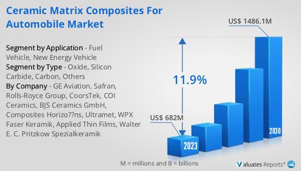
The aerospace and defense industry remains a hub of innovation, driven by the urgent need for modernization and the rising significance of emerging technologies like artificial intelligence and unmanned systems. The global Ceramic Matrix Composites for Automobile market was valued at US$ 682 million in 2023 and is projected to reach US$ 1486.1 million by 2030, reflecting a compound annual growth rate (CAGR) of 11.9% during the forecast period from 2024 to 2030. This growth is indicative of the increasing demand for high-performance materials that can meet the stringent requirements of modern automotive applications. The adoption of CMCs in the automobile industry is fueled by their superior properties, such as high-temperature resistance, lightweight nature, and exceptional strength, which make them ideal for various automotive components. As the industry continues to innovate and evolve, the role of CMCs in enhancing vehicle performance, efficiency, and sustainability is expected to become even more prominent.


Report Metric Details
Report Name Ceramic Matrix Composites for Automobile Market
Accounted market size in 2023 US$ 682 million
Forecasted market size in 2030 US$ 1486.1 million
CAGR 11.9%
Base Year 2023
Forecasted years 2024 - 2030
Segment by Type
  • Oxide
  • Silicon Carbide
  • Carbon
  • Others
Segment by Application
  • Fuel Vehicle
  • New Energy Vehicle
Production by Region
  • North America
  • Europe
  • China
  • Japan
Consumption by Region
  • North America (United States, Canada)
  • Europe (Germany, France, UK, Italy, Russia)
  • Asia-Pacific (China, Japan, South Korea, Taiwan)
  • Southeast Asia (India)
  • Latin America (Mexico, Brazil)
By Company GE Aviation, Safran, Rolls-Royce Group, CoorsTek, COI Ceramics, BJS Ceramics GmbH, Composites Horizo??ns, Ultramet, WPX Faser Keramik, Applied Thin Films, Walter E. C. Pritzkow Spezialkeramik
Forecast units USD million in value
Report coverage Revenue and volume forecast, company share, competitive landscape, growth factors and trends

Global Strong Cation Exchange Agarose Gel Market Research Report 2025

What is Global Strong Cation Exchange Agarose Gel Market? The Global Strong Cation Exchange Agarose Gel Market is a specialized segment wit...