What is Global Mobile Device Substrate-Like PCBs Market?
The Global Mobile Device Substrate-Like PCBs Market refers to the industry focused on the production and distribution of substrate-like printed circuit boards (PCBs) specifically designed for mobile devices. These PCBs are crucial components in mobile devices, providing the necessary infrastructure for electronic circuits to function efficiently. Substrate-like PCBs are known for their high density and fine line capabilities, which are essential for the compact and complex designs of modern mobile devices. They offer improved electrical performance, reliability, and miniaturization, making them ideal for smartphones, tablets, smartwatches, and other portable electronics. The market for these PCBs is driven by the increasing demand for advanced mobile devices with enhanced functionalities and the continuous trend towards miniaturization in the electronics industry. As mobile devices become more sophisticated, the need for high-performance PCBs that can support faster processing speeds, higher data transfer rates, and more efficient power management becomes critical. This market is characterized by rapid technological advancements and a competitive landscape, with manufacturers constantly innovating to meet the evolving needs of the mobile device industry. The growth of this market is also influenced by factors such as the proliferation of 5G technology, the rise of the Internet of Things (IoT), and the increasing consumer demand for smart and connected devices.
25/25µm and 30/30µm Line/Space, Less Than 25/25 µm Line/Space in the Global Mobile Device Substrate-Like PCBs Market:
In the realm of Global Mobile Device Substrate-Like PCBs Market, the specifications of line and space dimensions, such as 25/25µm and 30/30µm, play a pivotal role in defining the performance and capabilities of the PCBs. These measurements refer to the width of the conductive lines and the spaces between them on the PCB. A 25/25µm line/space indicates that both the line width and the space between lines are 25 micrometers, while a 30/30µm line/space means both are 30 micrometers. The trend towards smaller line/space dimensions, such as less than 25/25µm, is driven by the need for higher density interconnections and more compact designs in mobile devices. Smaller line/space dimensions allow for more circuitry to be packed into a smaller area, which is essential for the miniaturization of mobile devices. This miniaturization is crucial for accommodating the increasing number of features and functionalities in modern smartphones, tablets, and wearables. As consumers demand more powerful and feature-rich devices, manufacturers are compelled to adopt advanced PCB technologies that support finer line/space dimensions. The shift towards smaller line/space dimensions also enhances the electrical performance of the PCBs, as it reduces signal loss and improves the overall efficiency of the electronic circuits. This is particularly important in high-frequency applications, such as 5G communication, where signal integrity is paramount. The ability to produce PCBs with fine line/space dimensions is a testament to the advancements in manufacturing technologies and materials used in the PCB industry. It requires precision engineering and sophisticated fabrication processes to achieve the desired specifications without compromising on quality or reliability. The adoption of advanced materials, such as high-performance laminates and advanced copper foils, is also critical in achieving these fine dimensions. As the demand for smaller and more efficient PCBs continues to grow, manufacturers are investing in research and development to push the boundaries of what is possible in terms of line/space dimensions. This ongoing innovation is essential for keeping pace with the rapid advancements in mobile device technology and meeting the ever-evolving needs of consumers. The competition in the Global Mobile Device Substrate-Like PCBs Market is intense, with manufacturers striving to differentiate themselves by offering PCBs with superior performance, reliability, and cost-effectiveness. The ability to produce PCBs with smaller line/space dimensions is a key differentiator in this competitive landscape, as it directly impacts the performance and capabilities of the end devices. As a result, companies that can consistently deliver high-quality PCBs with fine line/space dimensions are well-positioned to capture a significant share of the market. The trend towards smaller line/space dimensions is expected to continue as mobile devices become more complex and feature-rich, driving the demand for advanced PCBs that can support these advancements. In conclusion, the specifications of line and space dimensions, such as 25/25µm and 30/30µm, are critical factors in the Global Mobile Device Substrate-Like PCBs Market. The push towards smaller dimensions is driven by the need for higher density interconnections, improved electrical performance, and the miniaturization of mobile devices. This trend is supported by advancements in manufacturing technologies and materials, as well as the ongoing innovation and competition in the PCB industry. As mobile devices continue to evolve, the demand for advanced PCBs with fine line/space dimensions is expected to grow, making this an exciting and dynamic area of the market.
Smart Phone, Smart Watch in the Global Mobile Device Substrate-Like PCBs Market:
The Global Mobile Device Substrate-Like PCBs Market plays a crucial role in the development and functionality of smart devices, particularly smartphones and smartwatches. In smartphones, substrate-like PCBs are essential for supporting the complex circuitry required for advanced features and functionalities. These PCBs provide the necessary infrastructure for integrating various components, such as processors, memory chips, and sensors, into a compact and efficient design. The high-density interconnections and fine line capabilities of substrate-like PCBs enable manufacturers to pack more features into smaller devices, meeting the consumer demand for sleek and powerful smartphones. The miniaturization of components facilitated by these PCBs also allows for longer battery life and improved performance, as they support efficient power management and faster data processing. In smartwatches, substrate-like PCBs are equally important, as they enable the integration of multiple functionalities into a small form factor. Smartwatches require compact and efficient PCBs to accommodate features such as fitness tracking, heart rate monitoring, GPS, and wireless connectivity. The fine line and space dimensions of substrate-like PCBs allow for the miniaturization of components, ensuring that smartwatches remain lightweight and comfortable to wear while offering a wide range of functionalities. The ability to integrate advanced features into a small and efficient design is a key factor driving the adoption of substrate-like PCBs in the smartwatch market. The demand for smartwatches with enhanced capabilities, such as health monitoring and mobile payment options, is increasing, and substrate-like PCBs provide the necessary support for these advancements. The use of substrate-like PCBs in both smartphones and smartwatches is driven by the need for high-performance, reliable, and cost-effective solutions that can support the rapid advancements in mobile technology. As consumers continue to demand more from their smart devices, manufacturers are turning to advanced PCB technologies to meet these expectations. The Global Mobile Device Substrate-Like PCBs Market is characterized by continuous innovation and competition, with manufacturers striving to develop PCBs that offer superior performance, reliability, and cost-effectiveness. The ability to produce high-quality PCBs that can support the complex and compact designs of modern smart devices is a key differentiator in this competitive landscape. In conclusion, the Global Mobile Device Substrate-Like PCBs Market is integral to the development and functionality of smartphones and smartwatches. These PCBs provide the necessary infrastructure for integrating advanced features and functionalities into compact and efficient designs. The demand for high-performance, reliable, and cost-effective PCBs is driven by the rapid advancements in mobile technology and the increasing consumer demand for smart and connected devices. As the market continues to evolve, the role of substrate-like PCBs in supporting the development of innovative and feature-rich smart devices is expected to grow.
Global Mobile Device Substrate-Like PCBs Market Outlook:
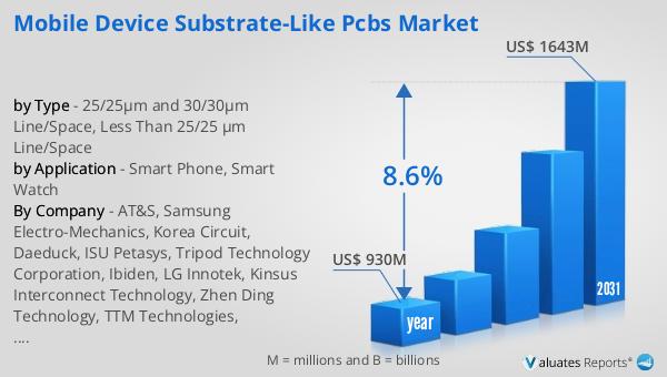
In 2024, the global market for Mobile Device Substrate-Like PCBs was valued at approximately $930 million. This market is anticipated to expand significantly, reaching an estimated size of $1,643 million by the year 2031. This growth trajectory represents a compound annual growth rate (CAGR) of 8.6% over the forecast period. The increasing demand for advanced mobile devices, coupled with the continuous trend towards miniaturization in the electronics industry, is driving this market expansion. As mobile devices become more sophisticated, the need for high-performance PCBs that can support faster processing speeds, higher data transfer rates, and more efficient power management becomes critical. The proliferation of 5G technology, the rise of the Internet of Things (IoT), and the increasing consumer demand for smart and connected devices are also contributing to the growth of this market. The competitive landscape of the Global Mobile Device Substrate-Like PCBs Market is characterized by rapid technological advancements and innovation, with manufacturers striving to develop PCBs that offer superior performance, reliability, and cost-effectiveness. As the market continues to evolve, the role of substrate-like PCBs in supporting the development of innovative and feature-rich mobile devices is expected to grow, making this an exciting and dynamic area of the market.
| Report Metric | Details |
| Report Name | Mobile Device Substrate-Like PCBs Market |
| Accounted market size in year | US$ 930 million |
| Forecasted market size in 2031 | US$ 1643 million |
| CAGR | 8.6% |
| Base Year | year |
| Forecasted years | 2025 - 2031 |
| by Type |
|
| by Application |
|
| Production by Region |
|
| Consumption by Region |
|
| By Company | AT&S, Samsung Electro-Mechanics, Korea Circuit, Daeduck, ISU Petasys, Tripod Technology Corporation, Ibiden, LG Innotek, Kinsus Interconnect Technology, Zhen Ding Technology, TTM Technologies, Unimicron |
| Forecast units | USD million in value |
| Report coverage | Revenue and volume forecast, company share, competitive landscape, growth factors and trends |


