What is Global GaN Wafers Market?
The Global GaN Wafers Market is a rapidly evolving sector within the semiconductor industry, focusing on the production and application of Gallium Nitride (GaN) wafers. GaN is a semiconductor material that has gained significant attention due to its superior properties compared to traditional silicon-based semiconductors. These properties include higher efficiency, greater thermal stability, and the ability to operate at higher voltages and frequencies. GaN wafers are primarily used in the manufacturing of electronic devices that require high power and high frequency, such as power amplifiers, radio frequency (RF) components, and light-emitting diodes (LEDs). The market for GaN wafers is driven by the increasing demand for energy-efficient electronic devices and the growing adoption of GaN technology in various applications, including telecommunications, automotive, and consumer electronics. As industries continue to seek more efficient and compact solutions, the demand for GaN wafers is expected to rise, making it a crucial component in the advancement of modern electronics. The market is characterized by continuous research and development efforts aimed at improving the quality and performance of GaN wafers, as well as reducing production costs to make them more accessible for widespread use.
2 inch GaN Substrate, 4 inch GaN Substrate, Others in the Global GaN Wafers Market:
In the Global GaN Wafers Market, substrates play a crucial role in determining the performance and efficiency of the final semiconductor devices. Among these substrates, the 2-inch GaN substrate is one of the most commonly used sizes. It is favored for its balance between cost and performance, making it suitable for a wide range of applications. The 2-inch substrate is often used in the production of LEDs and laser diodes, where its ability to handle high power densities and maintain stability under thermal stress is highly valued. This size is also popular in research and development settings, where smaller batches of wafers are needed for experimental purposes. On the other hand, the 4-inch GaN substrate is gaining popularity due to its larger surface area, which allows for the production of more devices per wafer. This size is particularly advantageous in high-volume manufacturing environments, where efficiency and cost-effectiveness are paramount. The 4-inch substrate is commonly used in the production of power electronic devices and RF components, where its larger size contributes to improved device performance and reduced production costs. Additionally, the larger substrate size facilitates the integration of more complex circuit designs, enabling the development of advanced electronic systems. Beyond the standard 2-inch and 4-inch substrates, the Global GaN Wafers Market also includes other substrate sizes and types, each catering to specific application needs. These may include custom-sized substrates for specialized applications or substrates made from alternative materials that offer unique properties. For instance, some manufacturers are exploring the use of silicon carbide (SiC) substrates in combination with GaN to enhance thermal conductivity and device performance. These alternative substrates are often used in niche applications where specific performance characteristics are required, such as in high-frequency or high-power electronic devices. The diversity of substrate options within the GaN Wafers Market reflects the wide range of applications and industries that rely on GaN technology. As the demand for more efficient and powerful electronic devices continues to grow, the development and adoption of various GaN substrate sizes and types are expected to expand, driving further innovation and growth in the market.
Laser Diodes, Power Electronic Devices, High Frequency Electronic Devices, Others in the Global GaN Wafers Market:
The Global GaN Wafers Market finds extensive usage across various applications, each benefiting from the unique properties of GaN technology. In the realm of laser diodes, GaN wafers are instrumental due to their ability to emit light in the blue and ultraviolet spectrum. This capability is crucial for applications such as Blu-ray players, data storage, and medical devices, where precise and efficient light emission is required. GaN-based laser diodes offer higher efficiency and longer lifespans compared to traditional semiconductor materials, making them a preferred choice in these industries. In power electronic devices, GaN wafers are revolutionizing the way energy is managed and utilized. Their high electron mobility and thermal stability allow for the development of power devices that are more efficient and compact than their silicon counterparts. This is particularly important in applications such as electric vehicles, renewable energy systems, and power supplies, where reducing energy loss and improving performance are critical. GaN-based power devices enable faster switching speeds and higher power densities, contributing to more efficient energy conversion and management. High-frequency electronic devices also benefit significantly from GaN technology. The ability of GaN wafers to operate at higher frequencies and voltages makes them ideal for RF and microwave applications, such as radar systems, satellite communications, and wireless networks. These devices require materials that can handle high power levels and maintain performance under demanding conditions, making GaN an excellent choice. Additionally, GaN technology is being explored in emerging applications such as 5G networks and advanced communication systems, where its high-frequency capabilities are essential for achieving the desired performance levels. Beyond these specific applications, GaN wafers are also used in a variety of other areas, including sensors, lighting, and electronic warfare systems. The versatility and superior performance of GaN technology make it a valuable component in the development of next-generation electronic devices across multiple industries. As the demand for more efficient, powerful, and compact electronic solutions continues to grow, the usage of GaN wafers in these and other applications is expected to expand, driving further innovation and growth in the market.
Global GaN Wafers Market Outlook:
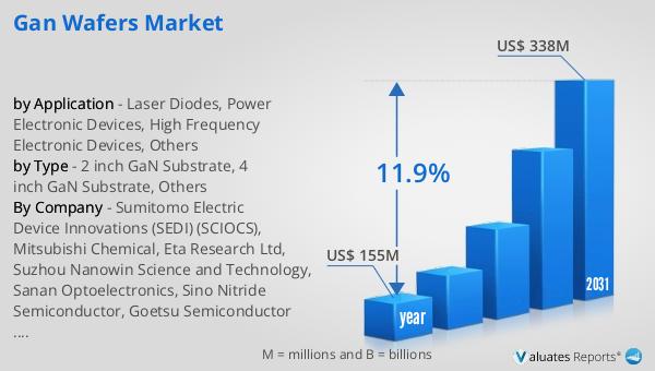
The global market for GaN Wafers was valued at approximately $155 million in 2024, and it is anticipated to experience significant growth over the coming years. By 2031, the market is projected to reach an estimated size of $338 million, reflecting a robust compound annual growth rate (CAGR) of 11.9% during the forecast period. This growth is driven by the increasing demand for GaN technology across various industries, including telecommunications, automotive, and consumer electronics. The superior properties of GaN wafers, such as higher efficiency, greater thermal stability, and the ability to operate at higher voltages and frequencies, make them an attractive choice for manufacturers seeking to develop more efficient and powerful electronic devices. As industries continue to prioritize energy efficiency and performance, the adoption of GaN wafers is expected to rise, contributing to the market's expansion. Additionally, ongoing research and development efforts aimed at improving the quality and performance of GaN wafers, as well as reducing production costs, are likely to further support market growth. The increasing availability of GaN wafers and the development of new applications are expected to drive demand and create new opportunities for growth in the global GaN Wafers Market.
| Report Metric | Details |
| Report Name | GaN Wafers Market |
| Accounted market size in year | US$ 155 million |
| Forecasted market size in 2031 | US$ 338 million |
| CAGR | 11.9% |
| Base Year | year |
| Forecasted years | 2025 - 2031 |
| by Type |
|
| by Application |
|
| Production by Region |
|
| Consumption by Region |
|
| By Company | Sumitomo Electric Device Innovations (SEDI) (SCIOCS), Mitsubishi Chemical, Eta Research Ltd, Suzhou Nanowin Science and Technology, Sanan Optoelectronics, Sino Nitride Semiconductor, Goetsu Semiconductor Wuxi, BTOZ, Toyoda Gosei, Kyma Technologies |
| Forecast units | USD million in value |
| Report coverage | Revenue and volume forecast, company share, competitive landscape, growth factors and trends |