What is Global Carborundum Wafer Market?
The Global Carborundum Wafer Market is a significant segment within the semiconductor industry, primarily driven by the increasing demand for high-performance electronic devices. Carborundum, also known as silicon carbide (SiC), is a compound that offers superior properties such as high thermal conductivity, high-temperature resistance, and excellent electrical characteristics. These properties make it an ideal material for manufacturing wafers used in various electronic applications. The market for carborundum wafers is expanding due to the growing need for energy-efficient devices and the rising adoption of electric vehicles, which require advanced power electronics. Additionally, the increasing deployment of 5G technology and the expansion of wireless infrastructure are further propelling the demand for carborundum wafers. As industries continue to seek materials that can withstand extreme conditions and deliver enhanced performance, the global carborundum wafer market is poised for substantial growth. The market's expansion is also supported by ongoing research and development efforts aimed at improving the quality and reducing the cost of carborundum wafers, making them more accessible for various applications. Overall, the global carborundum wafer market is a dynamic and rapidly evolving sector with significant potential for future growth.
4 Inch, 6 Inch, 8 Inch in the Global Carborundum Wafer Market:
In the Global Carborundum Wafer Market, the size of the wafer plays a crucial role in determining its application and efficiency. The most common sizes are 4-inch, 6-inch, and 8-inch wafers, each offering distinct advantages and catering to different segments of the market. The 4-inch wafers are typically used in niche applications where smaller devices are required. They are often favored in research and development settings due to their cost-effectiveness and ease of handling. Despite their smaller size, 4-inch wafers are capable of delivering high performance in specific applications, making them a valuable component in the semiconductor industry. On the other hand, 6-inch wafers are more widely used in industrial applications. They strike a balance between size and performance, offering a larger surface area for device fabrication while maintaining manageable production costs. The 6-inch wafers are commonly used in the production of power devices and other electronic components that require a moderate level of performance. Their versatility and cost-effectiveness make them a popular choice among manufacturers looking to optimize their production processes. The 8-inch wafers represent the largest size category in the carborundum wafer market. These wafers are primarily used in high-volume manufacturing environments where large-scale production is required. The increased surface area of 8-inch wafers allows for the fabrication of more devices per wafer, leading to improved economies of scale and reduced production costs. This makes them ideal for applications in power electronics and optoelectronics, where high performance and efficiency are critical. The use of 8-inch wafers is particularly prevalent in the production of advanced semiconductor devices, where the demand for high-quality materials is paramount. As the global carborundum wafer market continues to evolve, the demand for different wafer sizes will be influenced by technological advancements and changing industry requirements. Manufacturers are constantly exploring new ways to enhance the performance and reduce the cost of carborundum wafers, ensuring that they remain competitive in the ever-changing semiconductor landscape. The choice of wafer size ultimately depends on the specific needs of the application and the desired balance between performance, cost, and production efficiency. As such, the market for 4-inch, 6-inch, and 8-inch carborundum wafers is expected to remain diverse and dynamic, catering to a wide range of applications across various industries.
Power Device, Electronics & Optoelectronics, Wireless Infrastructure, Other in the Global Carborundum Wafer Market:
The Global Carborundum Wafer Market finds extensive usage across several key areas, including Power Devices, Electronics & Optoelectronics, Wireless Infrastructure, and other sectors. In the realm of Power Devices, carborundum wafers are highly valued for their ability to handle high voltages and temperatures, making them ideal for use in power converters, inverters, and other energy-efficient devices. The superior thermal conductivity and electrical properties of carborundum wafers enable the development of compact and efficient power devices that are crucial for applications in electric vehicles, renewable energy systems, and industrial automation. In the Electronics & Optoelectronics sector, carborundum wafers are used in the fabrication of high-performance semiconductors and optoelectronic components. Their ability to operate at high frequencies and temperatures makes them suitable for use in advanced electronic devices, including LEDs, laser diodes, and high-frequency transistors. The demand for carborundum wafers in this sector is driven by the need for faster, more efficient electronic components that can support the growing demand for high-speed data transmission and processing. In the Wireless Infrastructure domain, carborundum wafers play a critical role in the development of components for 5G networks and other wireless communication systems. The high-frequency capabilities of carborundum wafers make them ideal for use in RF amplifiers, filters, and other components that are essential for the deployment of next-generation wireless networks. As the demand for faster and more reliable wireless communication continues to grow, the use of carborundum wafers in this sector is expected to increase significantly. Beyond these primary areas, carborundum wafers are also used in a variety of other applications, including aerospace, defense, and telecommunications. Their unique properties make them suitable for use in harsh environments where traditional materials may fail. As industries continue to seek materials that can deliver enhanced performance and reliability, the global carborundum wafer market is poised for continued growth across a wide range of applications. The versatility and performance advantages of carborundum wafers make them a valuable component in the development of advanced technologies that are shaping the future of various industries.
Global Carborundum Wafer Market Outlook:
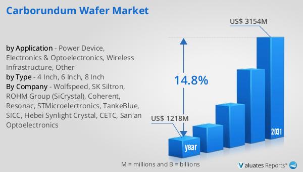
The global market for Carborundum Wafer was valued at $1,218 million in 2024 and is anticipated to grow significantly, reaching an estimated size of $3,154 million by 2031. This growth trajectory represents a compound annual growth rate (CAGR) of 14.8% over the forecast period. The robust growth of the carborundum wafer market can be attributed to several key factors. Firstly, the increasing demand for high-performance electronic devices is driving the need for advanced materials like carborundum wafers, which offer superior thermal and electrical properties. Additionally, the rising adoption of electric vehicles and the expansion of renewable energy systems are contributing to the growing demand for carborundum wafers in power electronics applications. Furthermore, the deployment of 5G technology and the expansion of wireless infrastructure are creating new opportunities for carborundum wafers in the telecommunications sector. As industries continue to seek materials that can withstand extreme conditions and deliver enhanced performance, the global carborundum wafer market is expected to experience substantial growth. The market's expansion is also supported by ongoing research and development efforts aimed at improving the quality and reducing the cost of carborundum wafers, making them more accessible for various applications. Overall, the global carborundum wafer market is a dynamic and rapidly evolving sector with significant potential for future growth.
| Report Metric | Details |
| Report Name | Carborundum Wafer Market |
| Accounted market size in year | US$ 1218 million |
| Forecasted market size in 2031 | US$ 3154 million |
| CAGR | 14.8% |
| Base Year | year |
| Forecasted years | 2025 - 2031 |
| by Type |
|
| by Application |
|
| Production by Region |
|
| Consumption by Region |
|
| By Company | Wolfspeed, SK Siltron, ROHM Group (SiCrystal), Coherent, Resonac, STMicroelectronics, TankeBlue, SICC, Hebei Synlight Crystal, CETC, San'an Optoelectronics |
| Forecast units | USD million in value |
| Report coverage | Revenue and volume forecast, company share, competitive landscape, growth factors and trends |