What is Global GaAs Wafer for VCSEL Market?
The Global GaAs Wafer for VCSEL Market refers to the worldwide industry focused on the production and application of Gallium Arsenide (GaAs) wafers specifically designed for Vertical-Cavity Surface-Emitting Lasers (VCSELs). GaAs is a compound semiconductor material that offers superior electron mobility and the ability to operate at higher frequencies compared to silicon, making it ideal for high-speed and optoelectronic applications. VCSELs, which are a type of semiconductor laser diode, emit light perpendicular to the surface of the wafer and are widely used in various applications due to their efficiency, reliability, and cost-effectiveness. The market for GaAs wafers for VCSELs is driven by the increasing demand for high-speed data transmission, advancements in consumer electronics, and the growing adoption of VCSELs in automotive and industrial applications. As industries continue to innovate and integrate more sophisticated technologies, the demand for GaAs wafers is expected to grow, supporting the development of faster and more efficient electronic and optoelectronic devices. This market is characterized by continuous research and development efforts aimed at improving wafer quality, reducing production costs, and expanding the range of applications for VCSELs.
2 inches, 4 inches, 6 inches, Others in the Global GaAs Wafer for VCSEL Market:
In the Global GaAs Wafer for VCSEL Market, the size of the wafer plays a crucial role in determining its application and efficiency. Wafers are typically categorized by their diameter, with common sizes being 2 inches, 4 inches, 6 inches, and others. Each size offers distinct advantages and is suited for different applications. The 2-inch GaAs wafers are often used in niche applications where smaller quantities of VCSELs are required. These wafers are easier to handle and are typically used in research and development settings or for specialized applications where the production scale is limited. The smaller size allows for precise control over the manufacturing process, which is essential for developing new technologies and prototypes. On the other hand, 4-inch GaAs wafers are more commonly used in commercial production environments. They offer a balance between size and cost, making them suitable for medium-scale production of VCSELs. The 4-inch wafers provide a larger surface area for device fabrication, which can lead to higher yields and more efficient production processes. This size is often preferred by manufacturers looking to produce VCSELs for consumer electronics and telecommunications applications, where moderate volumes are required. The 6-inch GaAs wafers represent a significant step up in terms of production capacity and efficiency. These larger wafers are used in high-volume manufacturing environments where the demand for VCSELs is substantial. The increased surface area of the 6-inch wafers allows for the production of a greater number of devices per wafer, reducing the overall cost per unit and improving the scalability of production. This size is particularly advantageous for applications in data centers and automotive industries, where large quantities of VCSELs are needed to support high-speed data transmission and advanced sensing technologies. Additionally, the category of "others" includes wafer sizes that are either smaller or larger than the standard sizes mentioned. These wafers are typically used for specialized applications or in industries where unique specifications are required. For instance, larger wafers may be used in industrial applications where high-power VCSELs are needed, while smaller wafers might be used in compact devices or systems with space constraints. The choice of wafer size is influenced by several factors, including the intended application, production volume, and cost considerations. Manufacturers must carefully evaluate these factors to select the appropriate wafer size that meets their specific needs while optimizing production efficiency and cost-effectiveness. As the demand for VCSELs continues to grow across various industries, the Global GaAs Wafer for VCSEL Market is expected to see increased diversification in wafer sizes to accommodate the evolving needs of different applications. This diversification will likely drive further innovation in wafer manufacturing processes and technologies, enabling the production of more advanced and efficient VCSELs.
Telecommunications, Consumer Electronics, Data Center, Commercial & Industrial, Automotive, Healthcare, Military in the Global GaAs Wafer for VCSEL Market:
The Global GaAs Wafer for VCSEL Market finds extensive usage across a variety of sectors, each benefiting from the unique properties of GaAs-based VCSELs. In telecommunications, VCSELs are integral to high-speed data transmission, enabling faster and more reliable communication networks. The ability of VCSELs to operate at high frequencies and their efficiency in converting electrical signals into optical signals make them ideal for fiber optic communications, where they facilitate the rapid transfer of large volumes of data over long distances. In consumer electronics, VCSELs are used in devices such as smartphones, tablets, and laptops, where they support features like facial recognition, gesture sensing, and proximity detection. The compact size and low power consumption of VCSELs make them well-suited for integration into portable electronic devices, enhancing user experience and device functionality. Data centers, which require high-speed and high-capacity data transmission, also rely heavily on VCSELs. The use of GaAs wafers in VCSELs allows for the development of lasers that can handle the massive data loads typical of modern data centers, ensuring efficient and reliable data processing and storage. In the commercial and industrial sectors, VCSELs are used in a range of applications, from barcode scanning to industrial automation. Their precision and reliability make them ideal for tasks that require accurate and consistent performance. The automotive industry is another significant user of VCSELs, where they are employed in advanced driver-assistance systems (ADAS), LiDAR, and other sensing technologies. The ability of VCSELs to provide accurate and real-time data is crucial for the development of autonomous vehicles and enhanced safety features. In healthcare, VCSELs are used in medical imaging and diagnostic equipment, where their precision and ability to operate at specific wavelengths enable detailed and accurate imaging. This is particularly important in applications such as optical coherence tomography (OCT), where high-resolution images of biological tissues are required. The military sector also benefits from the use of VCSELs, where they are used in applications such as range finding, target designation, and secure communications. The robustness and reliability of GaAs-based VCSELs make them suitable for use in harsh and demanding environments, where performance and durability are critical. Overall, the versatility and efficiency of GaAs wafers for VCSELs make them indispensable across a wide range of industries, driving innovation and enhancing the capabilities of modern technologies.
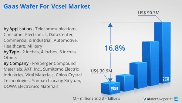
Global GaAs Wafer for VCSEL Market Outlook:
In 2024, the global market for GaAs Wafer for VCSEL was valued at approximately $30.9 million. This market is anticipated to experience significant growth over the coming years, with projections indicating that it will reach an estimated size of $90.3 million by 2031. This growth trajectory represents a compound annual growth rate (CAGR) of 16.8% during the forecast period. The increasing demand for high-speed data transmission, advancements in consumer electronics, and the growing adoption of VCSELs in various industries are key factors driving this market expansion. As industries continue to innovate and integrate more sophisticated technologies, the demand for GaAs wafers is expected to grow, supporting the development of faster and more efficient electronic and optoelectronic devices. This market is characterized by continuous research and development efforts aimed at improving wafer quality, reducing production costs, and expanding the range of applications for VCSELs. The robust growth prospects of the Global GaAs Wafer for VCSEL Market highlight the increasing importance of this technology in enabling the next generation of high-performance electronic and optoelectronic devices.
| Report Metric | Details |
| Report Name | GaAs Wafer for VCSEL Market |
| Accounted market size in year | US$ 30.9 million |
| Forecasted market size in 2031 | US$ 90.3 million |
| CAGR | 16.8% |
| Base Year | year |
| Forecasted years | 2025 - 2031 |
| by Type |
|
| by Application |
|
| Production by Region |
|
| Consumption by Region |
|
| By Company | Freiberger Compound Materials, AXT, Inc., Sumitomo Electric Industries, Vital Materials, China Crystal Technologies, Yunnan Lincang Xinyuan, DOWA Electronics Materials |
| Forecast units | USD million in value |
| Report coverage | Revenue and volume forecast, company share, competitive landscape, growth factors and trends |