What is Global GaAs Wafer for RF Devices Market?
The Global GaAs Wafer for RF Devices Market is a specialized segment within the semiconductor industry, focusing on the production and application of Gallium Arsenide (GaAs) wafers used in radio frequency (RF) devices. GaAs wafers are crucial components in the manufacturing of RF devices due to their superior electron mobility and ability to operate at higher frequencies compared to silicon-based wafers. These characteristics make GaAs wafers ideal for applications in wireless communication, satellite communication, and radar systems. The market is driven by the increasing demand for high-speed data transmission and the proliferation of wireless communication technologies. As the world becomes more connected, the need for efficient and reliable RF devices continues to grow, propelling the demand for GaAs wafers. The market is characterized by continuous technological advancements and innovations aimed at improving the performance and efficiency of RF devices. Companies operating in this market are investing heavily in research and development to enhance the quality and capabilities of GaAs wafers, thereby gaining a competitive edge. The Global GaAs Wafer for RF Devices Market is poised for significant growth, driven by the expanding telecommunications industry and the increasing adoption of advanced communication technologies.
2 inches, 3 inches, 4 inches, 6 inches, Others in the Global GaAs Wafer for RF Devices Market:
In the Global GaAs Wafer for RF Devices Market, the size of the wafer plays a crucial role in determining the efficiency and application of the RF devices. The market offers a variety of wafer sizes, including 2 inches, 3 inches, 4 inches, 6 inches, and others, each catering to specific needs and applications. The 2-inch GaAs wafers are typically used in niche applications where smaller devices are required. These wafers are often employed in research and development settings or in the production of specialized RF components that do not require large-scale manufacturing. Despite their limited size, 2-inch wafers are essential for certain applications where precision and compactness are paramount. Moving up in size, the 3-inch GaAs wafers are more commonly used in the production of RF devices for consumer electronics. These wafers offer a balance between size and efficiency, making them suitable for a wide range of applications, including mobile phones and wireless communication devices. The 3-inch wafers provide a larger surface area for device fabrication, allowing for increased production efficiency and cost-effectiveness. The 4-inch GaAs wafers are widely used in the telecommunications industry, particularly in the manufacturing of RF components for base stations and satellite communication systems. These wafers offer a significant increase in surface area compared to the smaller sizes, enabling the production of more complex and powerful RF devices. The 4-inch wafers are favored for their ability to support high-frequency operations and their compatibility with advanced manufacturing processes. The 6-inch GaAs wafers represent the largest standard size available in the market and are primarily used in high-volume manufacturing environments. These wafers are ideal for large-scale production of RF devices, offering the highest level of efficiency and cost-effectiveness. The 6-inch wafers are commonly used in the production of RF components for advanced communication systems, including 5G networks and satellite communication infrastructure. In addition to the standard sizes, the market also offers other wafer sizes to cater to specific customer requirements. These custom-sized wafers are often used in specialized applications where standard sizes do not meet the desired specifications. The availability of various wafer sizes in the Global GaAs Wafer for RF Devices Market ensures that manufacturers can choose the most suitable option for their specific needs, optimizing the performance and efficiency of their RF devices.
Power Amplifiers, RF Switches, Filters, Low Noise Amplifiers, Others in the Global GaAs Wafer for RF Devices Market:
The Global GaAs Wafer for RF Devices Market finds extensive usage in various applications, including power amplifiers, RF switches, filters, low noise amplifiers, and others. Power amplifiers are one of the primary applications of GaAs wafers in RF devices. These amplifiers are used to boost the power of RF signals, enabling them to travel longer distances without degradation. GaAs wafers are preferred for power amplifiers due to their high electron mobility and ability to operate at high frequencies, making them ideal for applications in wireless communication and broadcasting. RF switches are another critical application of GaAs wafers. These switches are used to route RF signals between different paths, allowing for efficient signal transmission and reception. GaAs wafers are favored for RF switches due to their low insertion loss and high isolation, ensuring minimal signal degradation and interference. Filters are essential components in RF devices, used to select or reject specific frequency bands. GaAs wafers are used in the production of RF filters due to their ability to operate at high frequencies and their excellent thermal stability. These characteristics make GaAs-based filters ideal for applications in telecommunications and satellite communication systems. Low noise amplifiers (LNAs) are used to amplify weak RF signals while minimizing the addition of noise. GaAs wafers are preferred for LNAs due to their low noise figure and high gain, ensuring clear and reliable signal amplification. These amplifiers are commonly used in applications such as radar systems and wireless communication devices. In addition to these primary applications, GaAs wafers are also used in other RF devices, including mixers, oscillators, and modulators. The versatility and superior performance of GaAs wafers make them indispensable in the production of a wide range of RF components, driving their demand in the Global GaAs Wafer for RF Devices Market.
Global GaAs Wafer for RF Devices Market Outlook:
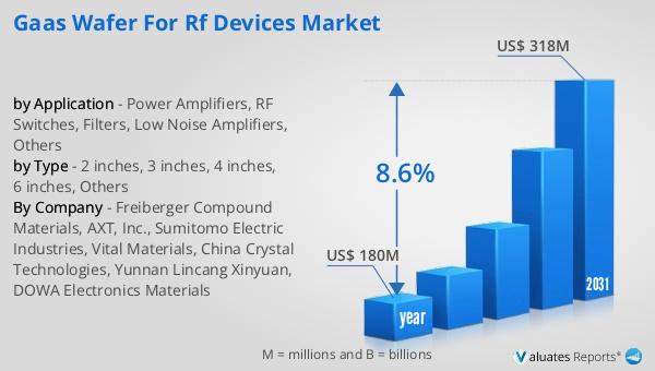
The global market for GaAs Wafer for RF Devices was valued at $180 million in 2024, with projections indicating a significant growth trajectory. By 2031, the market is expected to reach a revised size of $318 million, reflecting a compound annual growth rate (CAGR) of 8.6% during the forecast period. This growth is driven by the increasing demand for high-performance RF devices in various industries, including telecommunications, consumer electronics, and defense. The rising adoption of advanced communication technologies, such as 5G networks and satellite communication systems, is fueling the demand for GaAs wafers, as they offer superior performance and efficiency compared to traditional silicon-based wafers. The market's expansion is also supported by continuous technological advancements and innovations aimed at enhancing the capabilities of GaAs wafers. Companies operating in this market are investing heavily in research and development to improve the quality and performance of their products, thereby gaining a competitive edge. The growing emphasis on wireless communication and the need for efficient and reliable RF devices are expected to drive the demand for GaAs wafers in the coming years. As the market continues to evolve, manufacturers are focusing on developing new and improved GaAs wafers to meet the changing needs of the industry, ensuring sustained growth and profitability.
| Report Metric | Details |
| Report Name | GaAs Wafer for RF Devices Market |
| Accounted market size in year | US$ 180 million |
| Forecasted market size in 2031 | US$ 318 million |
| CAGR | 8.6% |
| Base Year | year |
| Forecasted years | 2025 - 2031 |
| by Type |
|
| by Application |
|
| Production by Region |
|
| Consumption by Region |
|
| By Company | Freiberger Compound Materials, AXT, Inc., Sumitomo Electric Industries, Vital Materials, China Crystal Technologies, Yunnan Lincang Xinyuan, DOWA Electronics Materials |
| Forecast units | USD million in value |
| Report coverage | Revenue and volume forecast, company share, competitive landscape, growth factors and trends |