Wednesday, March 5, 2025

Global Gas Sensor for Automotive Market Research Report 2025

What is Global Gas Sensor for Automotive Market?

The Global Gas Sensor for Automotive Market is a rapidly evolving sector that plays a crucial role in enhancing vehicle safety, efficiency, and environmental compliance. Gas sensors in automobiles are essential for detecting and measuring the concentration of various gases emitted by vehicles, such as carbon monoxide, nitrogen oxides, and hydrocarbons. These sensors are integral to the vehicle's emission control system, ensuring that the emissions remain within the regulatory limits set by governments worldwide. The market for these sensors is driven by the increasing demand for vehicles that meet stringent emission standards, the growing awareness of environmental issues, and the technological advancements in sensor technology. As automotive manufacturers strive to produce cleaner and more efficient vehicles, the demand for advanced gas sensors continues to rise. These sensors not only help in reducing harmful emissions but also contribute to improving the overall performance and fuel efficiency of vehicles. With the automotive industry undergoing a significant transformation towards electrification and hybridization, the role of gas sensors is becoming even more critical in ensuring that vehicles are both environmentally friendly and high-performing.

Gas Sensor for Automotive Market

Exhaust Gas Sensor, Intake Gas Sensor in the Global Gas Sensor for Automotive Market:

Exhaust gas sensors and intake gas sensors are two primary types of sensors used in the Global Gas Sensor for Automotive Market, each serving distinct yet complementary roles in vehicle operation. Exhaust gas sensors are primarily responsible for monitoring the gases emitted from the vehicle's exhaust system. These sensors play a pivotal role in ensuring that the emissions are within the permissible limits, thereby helping in reducing the environmental impact of vehicles. They detect harmful gases such as carbon monoxide (CO), nitrogen oxides (NOx), and hydrocarbons (HC), which are byproducts of the combustion process in the engine. By providing real-time data on the concentration of these gases, exhaust gas sensors enable the vehicle's engine control unit (ECU) to adjust the air-fuel mixture, ignition timing, and other parameters to optimize combustion efficiency and minimize emissions. This not only helps in meeting stringent emission regulations but also enhances the vehicle's fuel efficiency and performance. On the other hand, intake gas sensors are used to monitor the air entering the engine. These sensors measure parameters such as air mass flow, temperature, and pressure, which are critical for determining the optimal air-fuel ratio for combustion. By ensuring that the engine receives the right amount of air, intake gas sensors help in achieving efficient combustion, reducing fuel consumption, and minimizing emissions. They also play a crucial role in turbocharged engines, where precise control of the air intake is essential for maximizing performance and efficiency. Together, exhaust and intake gas sensors form an integral part of the vehicle's emission control system, working in tandem to ensure that the engine operates efficiently and cleanly. As the automotive industry continues to evolve, the demand for advanced gas sensors is expected to grow, driven by the need for vehicles that are both environmentally friendly and high-performing. With advancements in sensor technology, modern gas sensors are becoming more accurate, reliable, and capable of operating in harsh automotive environments. This is enabling automotive manufacturers to develop vehicles that not only meet but exceed emission standards, contributing to a cleaner and more sustainable future.

Passenger Vehicle, Commercial Vehicle in the Global Gas Sensor for Automotive Market:

The usage of gas sensors in the Global Gas Sensor for Automotive Market is particularly significant in two major vehicle categories: passenger vehicles and commercial vehicles. In passenger vehicles, gas sensors are primarily used to enhance the safety, efficiency, and environmental compliance of the vehicle. With the increasing awareness of environmental issues and the implementation of stringent emission regulations, automotive manufacturers are focusing on developing passenger vehicles that are both fuel-efficient and low-emission. Gas sensors play a crucial role in achieving this by providing real-time data on the concentration of various gases emitted by the vehicle. This data is used by the vehicle's engine control unit (ECU) to optimize combustion efficiency, reduce emissions, and improve fuel economy. In addition to emission control, gas sensors also contribute to the overall performance and safety of passenger vehicles by ensuring that the engine operates efficiently and reliably. In commercial vehicles, the role of gas sensors is even more critical due to the larger size and higher emission levels of these vehicles. Commercial vehicles, such as trucks and buses, are subject to stringent emission regulations, and non-compliance can result in significant penalties. Gas sensors help in ensuring that commercial vehicles meet these regulations by monitoring the emissions and providing real-time data to the vehicle's ECU. This enables the ECU to make necessary adjustments to the engine parameters, ensuring that the emissions remain within the permissible limits. Moreover, gas sensors also contribute to the fuel efficiency and performance of commercial vehicles by optimizing the combustion process. This is particularly important for commercial vehicles, as fuel costs constitute a significant portion of their operating expenses. By improving fuel efficiency, gas sensors help in reducing the overall operating costs of commercial vehicles, making them more economical and sustainable. Furthermore, with the increasing focus on reducing the carbon footprint of commercial vehicles, the demand for advanced gas sensors is expected to grow, driving the development of cleaner and more efficient commercial vehicles. Overall, the usage of gas sensors in both passenger and commercial vehicles is essential for meeting emission regulations, improving fuel efficiency, and enhancing vehicle performance, contributing to a cleaner and more sustainable automotive industry.

Global Gas Sensor for Automotive Market Outlook:

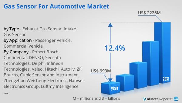
The global market for gas sensors in the automotive sector is experiencing significant growth, reflecting the increasing demand for vehicles that are both environmentally friendly and high-performing. In 2024, the market was valued at approximately $993 million, indicating a robust interest in these essential components. Looking ahead, the market is projected to expand substantially, reaching an estimated size of $2,226 million by 2031. This growth trajectory represents a compound annual growth rate (CAGR) of 12.4% over the forecast period. This impressive growth rate underscores the critical role that gas sensors play in the automotive industry, particularly as manufacturers strive to meet stringent emission standards and enhance vehicle efficiency. The rising awareness of environmental issues and the push for cleaner, more efficient vehicles are key drivers of this market expansion. As automotive technology continues to advance, the demand for sophisticated gas sensors that can accurately monitor and control emissions is expected to increase. This growth is not only a testament to the importance of gas sensors in modern vehicles but also highlights the ongoing transformation of the automotive industry towards sustainability and innovation. The market outlook for gas sensors in the automotive sector is indeed promising, with significant opportunities for growth and development in the coming years.


Report Metric Details
Report Name Gas Sensor for Automotive Market
Accounted market size in year US$ 993 million
Forecasted market size in 2031 US$ 2226 million
CAGR 12.4%
Base Year year
Forecasted years 2025 - 2031
by Type
  • Exhaust Gas Sensor
  • Intake Gas Sensor
by Application
  • Passenger Vehicle
  • Commercial Vehicle
Production by Region
  • North America
  • Europe
  • China
  • Japan
  • South Korea
Consumption by Region
  • North America (United States, Canada)
  • Europe (Germany, France, UK, Italy, Russia)
  • Asia-Pacific (China, Japan, South Korea, Taiwan)
  • Southeast Asia (India)
  • Latin America (Mexico, Brazil)
By Company Robert Bosch, Continental, DENSO, Sensata Technologies, Delphi, Infineon Technologies, Valeo, Hitachi, Autoliv, ZF, Bourns, Cubic Sensor and Instrument, Zhengzhou Weisheng Electronic, Hanwei Electronics Group, Luftmy Intelligence Technology
Forecast units USD million in value
Report coverage Revenue and volume forecast, company share, competitive landscape, growth factors and trends

Global Ceramic Coatings for Semiconductor Equipment Market Research Report 2025

What is Global Ceramic Coatings for Semiconductor Equipment Market?

The Global Ceramic Coatings for Semiconductor Equipment Market is a specialized segment within the broader semiconductor industry, focusing on the application of ceramic coatings to semiconductor manufacturing equipment. These coatings are crucial for enhancing the performance and longevity of equipment used in the production of semiconductors. Ceramic coatings provide a protective layer that can withstand high temperatures, corrosive environments, and mechanical wear, which are common in semiconductor manufacturing processes. This market is driven by the increasing demand for semiconductors across various industries, including electronics, automotive, and telecommunications. As technology advances, the need for more efficient and durable manufacturing equipment grows, leading to a higher demand for ceramic coatings. These coatings help in reducing maintenance costs and downtime, thereby improving the overall efficiency of semiconductor production. The market is characterized by continuous innovation, with companies investing in research and development to create advanced coatings that meet the evolving needs of the semiconductor industry. The growth of this market is also supported by the expansion of semiconductor manufacturing facilities worldwide, particularly in regions like Asia-Pacific, which is a major hub for semiconductor production.

Ceramic Coatings for Semiconductor Equipment Market

in the Global Ceramic Coatings for Semiconductor Equipment Market:

In the Global Ceramic Coatings for Semiconductor Equipment Market, various types of ceramic coatings are utilized by different customers based on their specific needs and applications. One of the most common types is alumina coatings, known for their excellent thermal stability and resistance to wear and corrosion. These coatings are widely used in semiconductor equipment that operates under high-temperature conditions, providing a protective barrier that extends the equipment's lifespan. Another popular type is yttria-stabilized zirconia (YSZ) coatings, which offer superior thermal insulation and are often used in environments where thermal shock resistance is critical. YSZ coatings are particularly beneficial in processes that involve rapid temperature changes, as they help prevent damage to the equipment. Silicon carbide coatings are also prevalent in the market, valued for their high hardness and chemical resistance. These coatings are ideal for equipment exposed to harsh chemical environments, as they provide a robust protective layer that minimizes the risk of corrosion and degradation. Additionally, titanium nitride coatings are used for their excellent wear resistance and low friction properties, making them suitable for components that experience significant mechanical stress. Customers in the semiconductor industry choose these coatings based on factors such as the specific manufacturing process, the operating environment, and the desired performance characteristics. For instance, in processes that involve aggressive chemicals, such as etching, silicon carbide coatings are preferred due to their chemical inertness. On the other hand, in applications where thermal management is crucial, such as thin film deposition, YSZ coatings are favored for their thermal insulation properties. The choice of coating also depends on the equipment's design and the materials used in its construction, as compatibility between the coating and the substrate is essential for optimal performance. Furthermore, the selection of ceramic coatings is influenced by the cost considerations and the expected return on investment. While advanced coatings may offer superior performance, they also come with a higher price tag, prompting customers to weigh the benefits against the costs. In some cases, customers may opt for a combination of different coatings to achieve the desired balance of performance and cost-effectiveness. The market is also seeing a trend towards the development of multifunctional coatings that combine the benefits of different materials, offering enhanced protection and performance in a single layer. This innovation is driven by the need to address the complex challenges faced by semiconductor manufacturers, such as increasing production efficiency and reducing downtime. As the semiconductor industry continues to evolve, the demand for specialized ceramic coatings is expected to grow, with customers seeking solutions that meet their specific requirements and contribute to the overall success of their manufacturing operations.

Etching, Thin Film, Others in the Global Ceramic Coatings for Semiconductor Equipment Market:

The usage of Global Ceramic Coatings for Semiconductor Equipment Market in areas such as etching, thin film, and others is pivotal to the efficiency and effectiveness of semiconductor manufacturing processes. In the etching process, ceramic coatings play a crucial role in protecting equipment from the aggressive chemicals used to remove material from the semiconductor wafer. These coatings provide a barrier that prevents corrosion and degradation, ensuring the longevity and reliability of the equipment. Silicon carbide coatings are particularly favored in etching applications due to their excellent chemical resistance and durability. By minimizing the wear and tear on equipment, these coatings help reduce maintenance costs and downtime, contributing to increased productivity and cost savings for manufacturers. In the thin film deposition process, ceramic coatings are essential for managing thermal conditions and ensuring uniform film growth. Yttria-stabilized zirconia (YSZ) coatings are commonly used in this area for their superior thermal insulation properties, which help maintain the optimal temperature conditions required for thin film deposition. These coatings also provide a smooth surface that facilitates the even distribution of thin films, resulting in high-quality semiconductor devices. The use of ceramic coatings in thin film applications enhances the precision and consistency of the manufacturing process, leading to improved device performance and yield. Beyond etching and thin film, ceramic coatings are also used in other semiconductor manufacturing processes, such as chemical vapor deposition (CVD) and physical vapor deposition (PVD). In these processes, the coatings protect equipment from the high temperatures and reactive gases involved, ensuring stable and reliable operation. Alumina coatings are often used in CVD and PVD applications for their excellent thermal stability and resistance to wear and corrosion. These coatings help maintain the integrity of the equipment, reducing the risk of contamination and defects in the semiconductor devices. The versatility and effectiveness of ceramic coatings make them an indispensable component of semiconductor manufacturing, enabling manufacturers to meet the demands of a rapidly evolving industry. As technology advances and the complexity of semiconductor devices increases, the need for specialized coatings that can withstand the rigors of modern manufacturing processes will continue to grow. Manufacturers are increasingly looking for coatings that offer a combination of properties, such as thermal stability, chemical resistance, and mechanical strength, to address the diverse challenges they face. The development of new and innovative ceramic coatings is expected to play a key role in the future of semiconductor manufacturing, providing the solutions needed to achieve higher levels of efficiency, quality, and performance.

Global Ceramic Coatings for Semiconductor Equipment Market Outlook:

The global market for ceramic coatings used in semiconductor equipment was valued at $745 million in 2024, with projections indicating it will grow to a revised size of $1,174 million by 2031, reflecting a compound annual growth rate (CAGR) of 6.8% over the forecast period. Meanwhile, the broader semiconductor market was estimated at $526.8 billion in 2023 and is expected to reach $780.7 billion by 2030. Our research suggests that the global semiconductor manufacturing wafer fabrication market is anticipated to expand from $251.7 billion in 2023 to $506.5 billion by 2030, achieving a remarkable CAGR of 40.49% during the forecast period. These figures underscore the significant growth potential within the semiconductor industry, driven by increasing demand for advanced electronic devices and the continuous evolution of technology. The expansion of the ceramic coatings market is closely linked to the broader trends in semiconductor manufacturing, as these coatings are essential for enhancing the performance and durability of equipment used in the production of semiconductors. As the industry continues to innovate and develop new technologies, the demand for high-quality ceramic coatings is expected to rise, supporting the growth of the market and contributing to the overall advancement of semiconductor manufacturing.


Report Metric Details
Report Name Ceramic Coatings for Semiconductor Equipment Market
Accounted market size in year US$ 745 million
Forecasted market size in 2031 US$ 1174 million
CAGR 6.8%
Base Year year
Forecasted years 2025 - 2031
Segment by Technology
  • Plasma Spray Coating
  • PVD & ALD Method
Segment by Application
  • Etching
  • Thin Film
  • Others
By Region
  • North America (United States, Canada)
  • Europe (Germany, France, UK, Italy, Russia) Rest of Europe
  • Nordic Countries
  • Asia-Pacific (China, Japan, South Korea)
  • Southeast Asia (India, Australia)
  • Rest of Asia
  • Latin America (Mexico, Brazil)
  • Rest of Latin America
  • Middle East & Africa (Turkey, Saudi Arabia, UAE, Rest of MEA)
By Company UCT (Ultra Clean Holdings, Inc), Kurita (Pentagon Technologies), Enpro Industries (LeanTeq and NxEdge), TOCALO Co., Ltd., Mitsubishi Chemical (Cleanpart), KoMiCo, Cinos, Hansol IONES, WONIK QnC, Dftech, TOPWINTECH, FEMVIX, SEWON HARDFACING CO.,LTD, Frontken Corporation Berhad, KERTZ HIGH TECH, Hung Jie Technology Corporation, Oerlikon Balzers, Beneq, APS Materials, Inc., SilcoTek, Alumiplate, ASSET Solutions, Inc., Persys Group, Entegris, Inficon, Value Engineering Co., Ltd, HTCSolar, Jiangsu Kaiweitesi Semiconductor Technology Co., Ltd., HCUT Co., Ltd, Ferrotec (Anhui) Technology Development Co., Ltd, Shanghai Companion, Chongqing Genori Technology Co., Ltd, GRAND HITEK
Forecast units USD million in value
Report coverage Revenue and volume forecast, company share, competitive landscape, growth factors and trends

Global Medical Thermistor Market Research Report 2025

What is Global Medical Thermistor Market?

The Global Medical Thermistor Market is a specialized segment within the broader medical device industry, focusing on thermistors used in various medical applications. Thermistors are temperature-sensitive resistors that change resistance with temperature changes, making them ideal for precise temperature monitoring and control. In the medical field, these devices are crucial for applications such as patient monitoring, diagnostic equipment, and therapeutic devices. The market is driven by the increasing demand for advanced healthcare solutions, the growing prevalence of chronic diseases, and the need for accurate temperature measurement in medical procedures. As healthcare technology advances, the demand for reliable and efficient thermistors continues to grow, contributing to the expansion of the global medical thermistor market. The market is characterized by continuous innovation and development, with manufacturers focusing on enhancing the accuracy, reliability, and miniaturization of thermistors to meet the evolving needs of the healthcare industry. Overall, the Global Medical Thermistor Market plays a vital role in ensuring the safety and effectiveness of medical devices, ultimately improving patient outcomes and advancing healthcare delivery worldwide.

Medical Thermistor Market

NTC Thermistor, PTC Thermistor in the Global Medical Thermistor Market:

NTC (Negative Temperature Coefficient) and PTC (Positive Temperature Coefficient) thermistors are two primary types of thermistors used in the Global Medical Thermistor Market, each serving distinct purposes based on their unique properties. NTC thermistors decrease in resistance as temperature increases, making them highly sensitive and suitable for precise temperature measurements. They are commonly used in medical applications where accurate temperature monitoring is critical, such as in patient monitoring systems, incubators, and respiratory devices. The ability of NTC thermistors to provide rapid and accurate temperature readings makes them indispensable in situations where even slight temperature variations can have significant impacts on patient care and treatment outcomes. On the other hand, PTC thermistors increase in resistance with rising temperatures, which makes them ideal for applications requiring overcurrent protection and self-regulating heating elements. In the medical field, PTC thermistors are often used in devices that require controlled heating, such as blood warmers and dialysis machines. Their self-regulating properties ensure that the devices operate within safe temperature ranges, preventing overheating and ensuring patient safety. The choice between NTC and PTC thermistors in medical applications depends on the specific requirements of the device and the desired temperature control characteristics. Both types of thermistors are integral to the development of advanced medical devices, contributing to the overall growth and innovation within the Global Medical Thermistor Market. As the demand for more sophisticated and reliable medical devices continues to rise, the role of NTC and PTC thermistors becomes increasingly important, driving further research and development in this field. Manufacturers are constantly exploring new materials and technologies to enhance the performance and efficiency of thermistors, ensuring they meet the stringent standards and regulations of the healthcare industry. This ongoing innovation not only supports the growth of the Global Medical Thermistor Market but also plays a crucial role in advancing medical technology and improving patient care worldwide.

Medical Industry, Pharmaceutical Industry in the Global Medical Thermistor Market:

The Global Medical Thermistor Market finds extensive usage in both the medical and pharmaceutical industries, each benefiting from the unique properties of thermistors in different ways. In the medical industry, thermistors are primarily used for patient monitoring and diagnostic purposes. They are integral components in devices such as electronic thermometers, patient monitoring systems, and incubators, where accurate temperature measurement is crucial for patient safety and effective treatment. The ability of thermistors to provide precise and rapid temperature readings ensures that healthcare providers can monitor patients' vital signs accurately, enabling timely interventions and improving patient outcomes. Additionally, thermistors are used in therapeutic devices such as blood warmers and dialysis machines, where maintaining specific temperature ranges is essential for the safety and efficacy of treatments. In the pharmaceutical industry, thermistors play a critical role in ensuring the quality and safety of pharmaceutical products. They are used in temperature-controlled storage and transportation systems, where maintaining the integrity of temperature-sensitive drugs and vaccines is paramount. Thermistors help monitor and regulate the temperature within storage facilities and transport containers, ensuring that pharmaceutical products remain within specified temperature ranges throughout the supply chain. This is particularly important for vaccines and biologics, which can lose their efficacy if exposed to temperatures outside their recommended storage conditions. The use of thermistors in the pharmaceutical industry not only helps maintain product quality but also ensures compliance with regulatory standards, ultimately safeguarding public health. Overall, the Global Medical Thermistor Market is essential for both the medical and pharmaceutical industries, providing the necessary tools for accurate temperature monitoring and control, which are critical for patient safety, treatment efficacy, and product quality.

Global Medical Thermistor Market Outlook:

Based on our research, the global market for medical devices is projected to reach approximately $603 billion in 2023, with an anticipated growth rate of 5% annually over the next six years. This growth is indicative of the increasing demand for advanced medical technologies and the continuous innovation within the healthcare sector. The expansion of the medical device market is driven by several factors, including the rising prevalence of chronic diseases, an aging global population, and the growing emphasis on improving healthcare infrastructure worldwide. As healthcare systems strive to enhance patient care and outcomes, the demand for sophisticated medical devices, including thermistors, is expected to rise. Thermistors, with their critical role in temperature monitoring and control, are integral to the development and functionality of many medical devices. Their ability to provide precise and reliable temperature measurements ensures the safety and effectiveness of medical treatments, contributing to the overall growth of the medical device market. As the market continues to expand, manufacturers are focusing on developing innovative thermistor technologies to meet the evolving needs of the healthcare industry, ultimately driving further advancements in medical technology and improving patient care globally.


Report Metric Details
Report Name Medical Thermistor Market
Accounted market size in year US$ 603 billion
CAGR 5%
Base Year year
by Type
  • NTC Thermistor
  • PTC Thermistor
by Application
  • Medical Industry
  • Pharmaceutical Industry
Production by Region
  • North America
  • Europe
  • China
  • Japan
  • South Korea
Consumption by Region
  • North America (United States, Canada)
  • Europe (Germany, France, UK, Italy, Russia)
  • Asia-Pacific (China, Japan, South Korea, Taiwan)
  • Southeast Asia (India)
  • Latin America (Mexico, Brazil)
By Company Temperature Specialists, Inc., Tempco Electric Heater Corp., Minco, Quality Thermistor, Inc., Therm-X, Ametherm, Inc., Sensor Scientific, Inc.
Forecast units USD million in value
Report coverage Revenue and volume forecast, company share, competitive landscape, growth factors and trends

Global Copper Polishing Slurry Market Research Report 2025

What is Global Copper Polishing Slurry Market?

The Global Copper Polishing Slurry Market is a specialized segment within the broader semiconductor industry, focusing on the materials used in the chemical mechanical planarization (CMP) process. CMP is a critical step in semiconductor manufacturing, where a slurry is used to smooth and flatten the surface of semiconductor wafers, particularly those made of copper. This process is essential for creating the intricate patterns required for modern electronic devices. The slurry typically consists of abrasive particles suspended in a chemical solution, which helps to remove excess material and achieve the desired surface finish. The demand for copper polishing slurry is driven by the increasing complexity of semiconductor devices and the need for higher performance and miniaturization. As technology advances, the requirements for precision and efficiency in the CMP process become more stringent, leading to innovations in slurry formulations. The market is characterized by a focus on developing slurries that offer improved removal rates, selectivity, and defectivity, while also being environmentally friendly. This market is poised for growth as the semiconductor industry continues to expand, driven by the proliferation of electronic devices and the ongoing development of new technologies.

Copper Polishing Slurry Market

Colloidal Silica Based Slurry, Alumina Based Slurry in the Global Copper Polishing Slurry Market:

Colloidal silica-based slurry and alumina-based slurry are two prominent types of slurries used in the Global Copper Polishing Slurry Market, each with distinct characteristics and applications. Colloidal silica-based slurry is known for its fine particle size and uniform distribution, which makes it ideal for achieving a high-quality surface finish with minimal defects. The silica particles are suspended in a chemical solution that facilitates the removal of excess copper material during the CMP process. This type of slurry is particularly effective in applications where a smooth and defect-free surface is critical, such as in the production of advanced semiconductor devices. The chemical composition of colloidal silica-based slurry can be tailored to enhance its performance, allowing for precise control over the polishing process. On the other hand, alumina-based slurry is characterized by its harder abrasive particles, which provide a higher removal rate compared to colloidal silica-based slurry. This makes it suitable for applications where rapid material removal is necessary, such as in the initial stages of the CMP process. Alumina-based slurry is often used in conjunction with other types of slurries to achieve the desired balance between removal rate and surface finish. The choice between colloidal silica-based and alumina-based slurry depends on the specific requirements of the application, including the type of semiconductor device being manufactured and the desired surface characteristics. Both types of slurries play a crucial role in the CMP process, contributing to the overall efficiency and effectiveness of semiconductor manufacturing. As the demand for more advanced and miniaturized electronic devices continues to grow, the development of new and improved slurry formulations will be essential to meet the evolving needs of the industry.

Logic Chips, Memory Chips, Advanced Packaging in the Global Copper Polishing Slurry Market:

The Global Copper Polishing Slurry Market plays a vital role in the production of various semiconductor components, including logic chips, memory chips, and advanced packaging. Logic chips, which are used to perform the processing functions in electronic devices, require a high degree of precision and accuracy during manufacturing. The CMP process, facilitated by copper polishing slurry, is essential for creating the intricate patterns and structures needed for these chips to function effectively. The slurry helps to achieve the necessary surface planarity and smoothness, ensuring that the logic chips can operate at high speeds and with minimal power consumption. Memory chips, which are used to store data in electronic devices, also benefit from the use of copper polishing slurry. The CMP process helps to create the fine structures required for high-density memory storage, allowing for greater data capacity and faster access times. The use of copper polishing slurry in the production of memory chips is critical for meeting the increasing demand for more powerful and efficient storage solutions. Advanced packaging, which involves the integration of multiple semiconductor components into a single package, also relies on the CMP process and copper polishing slurry. This process is essential for ensuring the proper alignment and connection of the various components, which is crucial for the performance and reliability of the final product. The use of copper polishing slurry in advanced packaging helps to achieve the necessary surface finish and planarity, enabling the production of more compact and efficient electronic devices. As the semiconductor industry continues to evolve, the role of copper polishing slurry in the production of logic chips, memory chips, and advanced packaging will remain critical, driving further innovation and development in this market.

Global Copper Polishing Slurry Market Outlook:

In 2024, the global market for Copper Polishing Slurry was valued at approximately $540 million, and it is anticipated to grow to a revised size of $798 million by 2031, reflecting a compound annual growth rate (CAGR) of 5.8% over the forecast period. This growth is indicative of the increasing demand for advanced semiconductor devices and the critical role that copper polishing slurry plays in their production. The broader semiconductor market was estimated at $526.8 billion in 2023 and is projected to reach $780.7 billion by 2030. This expansion underscores the rapid advancements in technology and the growing need for more sophisticated electronic components. Additionally, the global semiconductor manufacturing wafer fabrication market is expected to grow from $251.7 billion in 2023 to $506.5 billion by 2030, with a remarkable CAGR of 40.49% during the forecast period. This significant growth highlights the importance of copper polishing slurry in the semiconductor manufacturing process, as it is essential for achieving the precision and quality required for modern electronic devices. The continued development and innovation in slurry formulations will be crucial for supporting the evolving needs of the semiconductor industry and maintaining the momentum of market growth.


Report Metric Details
Report Name Copper Polishing Slurry Market
Accounted market size in year US$ 540 million
Forecasted market size in 2031 US$ 798 million
CAGR 5.8%
Base Year year
Forecasted years 2025 - 2031
by Type
  • Colloidal Silica Based Slurry
  • Alumina Based Slurry
by Application
  • Logic Chips
  • Memory Chips
  • Advanced Packaging
Production by Region
  • North America
  • Europe
  • China
  • Japan
  • South Korea
Consumption by Region
  • North America (United States, Canada)
  • Europe (Germany, France, UK, Italy, Russia)
  • Asia-Pacific (China, Japan, South Korea, Taiwan)
  • Southeast Asia (India)
  • Latin America (Mexico, Brazil)
By Company Fujifilm, Resonac, FUJIMI INCORPORATED, DuPont, Merck (Versum Materials), Anjimirco Shanghai, Soulbrain, Saint-Gobain, Vibrantz (Ferro), TOPPAN INFOMEDIA CO., LTD, Samsung SDI
Forecast units USD million in value
Report coverage Revenue and volume forecast, company share, competitive landscape, growth factors and trends

Global CMP Tungsten Polishing Fluid Market Research Report 2025

What is Global CMP Tungsten Polishing Fluid Market?

The Global CMP Tungsten Polishing Fluid Market is a specialized segment within the semiconductor industry, focusing on the chemical mechanical planarization (CMP) process. CMP is a critical step in semiconductor manufacturing, used to smooth and flatten the surface of semiconductor wafers. Tungsten polishing fluids are specifically designed for the CMP of tungsten, a metal commonly used in semiconductor devices for its excellent electrical conductivity and thermal properties. These fluids are formulated with a combination of chemicals and abrasives that work together to remove excess material and achieve the desired surface finish. The demand for CMP tungsten polishing fluids is driven by the increasing complexity of semiconductor devices, which require precise and uniform surfaces to function effectively. As technology advances, the need for high-performance polishing fluids that can deliver consistent results becomes even more crucial. The market is characterized by continuous innovation, with manufacturers striving to develop formulations that offer improved performance, reduced environmental impact, and cost-effectiveness. The growth of the semiconductor industry, particularly in regions like Asia-Pacific, further fuels the demand for these specialized fluids, making the Global CMP Tungsten Polishing Fluid Market a dynamic and evolving sector.

CMP Tungsten Polishing Fluid Market

in the Global CMP Tungsten Polishing Fluid Market:

The Global CMP Tungsten Polishing Fluid Market caters to a diverse range of customers, each with specific requirements based on their applications and technological needs. These fluids are primarily used by semiconductor manufacturers, who rely on them to achieve the precise surface planarization required for advanced semiconductor devices. The types of CMP tungsten polishing fluids vary based on their chemical composition, abrasive content, and intended application. Some fluids are designed for high removal rates, making them suitable for applications where rapid material removal is necessary. These are often used in the initial stages of the CMP process, where large amounts of material need to be removed quickly. Other fluids are formulated for low defectivity, focusing on minimizing surface defects and achieving a high-quality finish. These are typically used in the final stages of polishing, where precision and surface quality are paramount. Additionally, there are fluids specifically designed for use with certain types of equipment or processes, such as those compatible with specific polishing pads or slurry delivery systems. The choice of fluid depends on various factors, including the type of semiconductor device being manufactured, the specific requirements of the CMP process, and the desired balance between performance and cost. For instance, manufacturers of DRAM and 3D NAND devices may prioritize high removal rates to meet the demands of high-volume production, while those producing logic ICs might focus on achieving the highest possible surface quality to ensure optimal device performance. The market also sees a demand for environmentally friendly formulations, as manufacturers seek to reduce the environmental impact of their processes. This has led to the development of polishing fluids that use less hazardous chemicals and generate less waste, aligning with broader industry trends towards sustainability. Furthermore, the market is influenced by regional variations, with different regions exhibiting distinct preferences and requirements based on their local semiconductor industries. In Asia-Pacific, for example, the rapid growth of the semiconductor sector drives a high demand for advanced CMP solutions, while in North America and Europe, there may be a greater emphasis on innovation and the development of next-generation technologies. Overall, the Global CMP Tungsten Polishing Fluid Market is characterized by a wide range of products tailored to meet the diverse needs of its customers, reflecting the complexity and dynamism of the semiconductor industry.

DRAM, 3D NAND, Logic IC, Others in the Global CMP Tungsten Polishing Fluid Market:

The usage of Global CMP Tungsten Polishing Fluid Market extends across various areas of semiconductor manufacturing, including DRAM, 3D NAND, Logic IC, and others. In the production of DRAM (Dynamic Random-Access Memory), CMP tungsten polishing fluids play a crucial role in ensuring the smooth and uniform surfaces required for efficient memory cell operation. DRAM devices are characterized by their high density and need for rapid data access, which necessitates precise manufacturing processes. The polishing fluids used in DRAM production are typically formulated to achieve high removal rates and low defectivity, balancing speed and quality to meet the demands of high-volume manufacturing. In the case of 3D NAND, a type of non-volatile memory that stacks memory cells vertically to increase storage capacity, CMP tungsten polishing fluids are essential for creating the intricate multi-layer structures. The fluids used in 3D NAND production must be capable of handling the complex geometries and tight tolerances associated with these advanced devices. They are often designed to provide excellent planarization and surface finish, ensuring the reliability and performance of the final product. For Logic ICs (Integrated Circuits), which are used in a wide range of applications from consumer electronics to industrial systems, CMP tungsten polishing fluids are critical for achieving the high levels of precision and surface quality required for optimal device performance. Logic ICs often involve complex circuit designs and require polishing fluids that can deliver consistent results across different layers and materials. The fluids used in this area are typically formulated to minimize defects and ensure uniformity, supporting the production of high-performance and reliable devices. Beyond these specific applications, CMP tungsten polishing fluids are also used in other areas of semiconductor manufacturing, such as the production of microprocessors, sensors, and other advanced electronic components. In these applications, the choice of polishing fluid is influenced by factors such as the specific materials being processed, the desired surface characteristics, and the overall manufacturing goals. As the semiconductor industry continues to evolve, the demand for high-performance CMP tungsten polishing fluids is expected to grow, driven by the increasing complexity and sophistication of semiconductor devices.

Global CMP Tungsten Polishing Fluid Market Outlook:

In 2024, the global market for CMP Tungsten Polishing Fluid was valued at approximately $586 million. By 2031, it is anticipated to expand to a revised size of $975 million, reflecting a compound annual growth rate (CAGR) of 7.7% over the forecast period. Meanwhile, the broader semiconductor market was estimated at $526.8 billion in 2023 and is projected to reach $780.7 billion by 2030. Our research indicates that the global semiconductor manufacturing wafer fabrication market is expected to grow significantly, from $251.7 billion in 2023 to $506.5 billion by 2030, with a remarkable CAGR of 40.49% during this period. These projections underscore the robust growth and dynamic nature of the semiconductor industry, driven by technological advancements and increasing demand for electronic devices. The CMP Tungsten Polishing Fluid Market, as a critical component of semiconductor manufacturing, is poised to benefit from these trends, with manufacturers focusing on innovation and efficiency to meet the evolving needs of the industry. The growth in wafer fabrication, in particular, highlights the increasing complexity and sophistication of semiconductor devices, necessitating advanced CMP solutions to ensure high-quality production. As the market continues to expand, companies are likely to invest in research and development to enhance the performance and sustainability of their polishing fluids, aligning with broader industry trends towards innovation and environmental responsibility.


Report Metric Details
Report Name CMP Tungsten Polishing Fluid Market
Accounted market size in year US$ 586 million
Forecasted market size in 2031 US$ 975 million
CAGR 7.7%
Base Year year
Forecasted years 2025 - 2031
by Application
  • DRAM
  • 3D NAND
  • Logic IC
  • Others
Production by Region
  • North America
  • South Korea
  • China
  • Japan
  • China Taiwan
Consumption by Region
  • North America (United States, Canada)
  • Europe (Germany, France, UK, Italy, Russia)
  • Asia-Pacific (China, Japan, South Korea, Taiwan)
  • Southeast Asia (India)
  • Latin America (Mexico, Brazil)
By Company Fujifilm, DuPont, Merck KGaA (Versum Materials), KC Tech, Dongjin Semichem, Anjimirco Shanghai, Samsung SDI, JSR Corporation, Vibrantz (Ferro), Hubei Dinglong, by Abrasive Type, Fumed Silica, High Purity Colloidal Silica
Forecast units USD million in value
Report coverage Revenue and volume forecast, company share, competitive landscape, growth factors and trends

Global Semiconductor Silicon Polishing Wafer Market Research Report 2025

What is Global Semiconductor Silicon Polishing Wafer Market?

The Global Semiconductor Silicon Polishing Wafer Market is a crucial segment within the semiconductor industry, focusing on the production and refinement of silicon wafers. These wafers are thin slices of semiconductor material, primarily silicon, which serve as the foundational substrate for fabricating integrated circuits and other microdevices. The market encompasses various processes and technologies aimed at enhancing the quality and performance of these wafers, including polishing, which is essential for achieving the smooth, defect-free surfaces required for advanced electronic applications. As the demand for smaller, more powerful, and energy-efficient electronic devices continues to grow, the need for high-quality silicon wafers has become increasingly critical. This market is driven by technological advancements, increased production capacities, and the expanding applications of semiconductors in various industries, including consumer electronics, automotive, telecommunications, and artificial intelligence. The global semiconductor silicon polishing wafer market is characterized by intense competition among key players, continuous innovation, and a focus on sustainability and cost-effectiveness. As a result, companies are investing heavily in research and development to improve wafer quality and production efficiency, ensuring they meet the evolving needs of the semiconductor industry.

Semiconductor Silicon Polishing Wafer Market

Less than 150 mm, 200 mm, 300 mm, Other(450 mm) in the Global Semiconductor Silicon Polishing Wafer Market:

In the Global Semiconductor Silicon Polishing Wafer Market, wafers are categorized based on their diameter, which significantly impacts their application and production processes. Wafers less than 150 mm in diameter are typically used in niche applications and older semiconductor technologies. These smaller wafers are often employed in the production of discrete components and specialized devices where the demand for high-volume production is lower. Despite their limited use in cutting-edge technologies, they remain essential for certain legacy systems and specific industrial applications. Moving to 200 mm wafers, these have been a staple in the semiconductor industry for many years. They are widely used in the production of a variety of semiconductor devices, including microcontrollers, sensors, and analog devices. The 200 mm wafers strike a balance between cost and performance, making them suitable for a broad range of applications, particularly in consumer electronics and automotive industries. As the industry progresses, the demand for 200 mm wafers continues to be strong, driven by the need for more sophisticated electronic components in everyday devices. The 300 mm wafers represent the current standard for high-volume semiconductor manufacturing. These larger wafers allow for more chips to be produced per wafer, significantly reducing the cost per chip and increasing production efficiency. The transition to 300 mm wafers has been driven by the need for higher performance and lower costs in the production of advanced semiconductor devices, such as microprocessors and memory chips. The use of 300 mm wafers is prevalent in the production of cutting-edge technologies, including those used in smartphones, data centers, and high-performance computing. Finally, the category of "Other" includes wafers with diameters of 450 mm and beyond. While still in the developmental and experimental stages, these larger wafers hold the potential to revolutionize the semiconductor industry by further reducing costs and increasing production efficiency. However, the transition to 450 mm wafers presents significant technical and economic challenges, requiring substantial investment in new manufacturing equipment and processes. Despite these challenges, the potential benefits of 450 mm wafers continue to drive research and development efforts, as the industry seeks to meet the growing demand for more powerful and cost-effective semiconductor solutions.

Electronic communication, Consumer Electronics, Artificial Intelligence, Other in the Global Semiconductor Silicon Polishing Wafer Market:

The Global Semiconductor Silicon Polishing Wafer Market plays a pivotal role in various sectors, including electronic communication, consumer electronics, artificial intelligence, and other emerging fields. In electronic communication, silicon wafers are fundamental in the production of integrated circuits used in communication devices such as smartphones, tablets, and networking equipment. The demand for faster and more reliable communication technologies drives the need for high-quality wafers that can support advanced functionalities and higher data transfer rates. In consumer electronics, silicon wafers are essential for manufacturing a wide range of devices, from televisions and gaming consoles to wearable technology and smart home devices. The continuous evolution of consumer electronics, with a focus on miniaturization and enhanced performance, necessitates the use of superior silicon wafers that can accommodate complex circuitry and high-density integration. In the realm of artificial intelligence, silicon wafers are crucial for developing powerful processors and specialized chips that enable machine learning and data processing capabilities. As AI technologies become more prevalent across industries, the demand for advanced semiconductor solutions, including high-performance silicon wafers, is expected to grow. Beyond these areas, the Global Semiconductor Silicon Polishing Wafer Market also supports other sectors such as automotive, healthcare, and industrial automation. In the automotive industry, silicon wafers are used in the production of sensors, microcontrollers, and other electronic components that are integral to modern vehicles' safety, efficiency, and connectivity features. In healthcare, semiconductor devices play a vital role in medical imaging, diagnostics, and wearable health monitoring systems, all of which rely on high-quality silicon wafers for their operation. Industrial automation, too, benefits from the advancements in semiconductor technology, with silicon wafers being used in the development of control systems, robotics, and other automated solutions. As these industries continue to evolve and expand, the Global Semiconductor Silicon Polishing Wafer Market is poised to play an increasingly important role in supporting technological innovation and meeting the growing demand for advanced electronic solutions.

Global Semiconductor Silicon Polishing Wafer Market Outlook:

The outlook for the Global Semiconductor Silicon Polishing Wafer Market is promising, with significant growth anticipated over the coming years. In 2022, the global semiconductor market was valued at approximately $579 billion, and it is projected to reach $790 billion by 2029, reflecting a compound annual growth rate (CAGR) of 6% during the forecast period. This growth is driven by several factors, including the increasing demand for semiconductors in various applications, such as consumer electronics, automotive, telecommunications, and artificial intelligence. As technology continues to advance, the need for more powerful, efficient, and cost-effective semiconductor solutions is expected to rise, further fueling the market's expansion. Additionally, the ongoing development of new technologies, such as 5G, the Internet of Things (IoT), and advanced driver-assistance systems (ADAS), is expected to create new opportunities for the semiconductor industry, driving demand for high-quality silicon wafers. As a result, companies within the Global Semiconductor Silicon Polishing Wafer Market are likely to continue investing in research and development to enhance wafer quality, production efficiency, and sustainability, ensuring they remain competitive in this rapidly evolving industry.


Report Metric Details
Report Name Semiconductor Silicon Polishing Wafer Market
Accounted market size in year US$ 579 billion
Forecasted market size in 2029 US$ 790 billion
CAGR 6%
Base Year year
Forecasted years 2025 - 2029
by Type
  • Less than 150 mm
  • 200 mm
  • 300 mm
  • Other(450 mm)
by Application
  • Electronic communication
  • Consumer Electronics
  • Artificial Intelligence
  • Other
Production by Region
  • North America
  • Europe
  • China
  • Japan
  • South Korea
Consumption by Region
  • North America (United States, Canada)
  • Europe (Germany, France, UK, Italy, Russia)
  • Asia-Pacific (China, Japan, South Korea, Taiwan)
  • Southeast Asia (India)
  • Latin America (Mexico, Brazil)
By Company Shin-Etsu Chemical, Sumco, Global Wafers, Siltronic, SK siltron, Waferworks, Ferrotec, AST, Gritek, Guosheng, QL Electronics, MCL, National Silicon Industry Group, GRINM Semiconductor Materials Co., Ltd., ThinkonSemi, Tianjin Zhonghuan Semiconducto, Hangzhou Leon Dongxin Microelectronics, Wafer Technology, Hangzhou Zhongxin Wafer Semiconductor, Tianjin Zhongjing Semiconductor Materials Co., Ltd., Suzhou New Micron Nano Technology, ESWIN
Forecast units USD million in value
Report coverage Revenue and volume forecast, company share, competitive landscape, growth factors and trends

Global Ferrite Multilayer Inductor Market Research Report 2025

What is Global Ferrite Multilayer Inductor Market?

The Global Ferrite Multilayer Inductor Market is a crucial segment within the electronics industry, characterized by its role in managing electrical currents and signals in various devices. Ferrite multilayer inductors are passive electronic components that store energy in a magnetic field when electric current flows through them. They are constructed using ferrite, a type of ceramic material that is highly effective in reducing electromagnetic interference. These inductors are essential in ensuring the smooth operation of electronic circuits by filtering noise and stabilizing voltage. The market for these components is driven by the increasing demand for miniaturized electronic devices, which require compact and efficient inductors. As technology advances, the need for high-performance inductors in applications such as smartphones, laptops, and other consumer electronics continues to grow. Additionally, the automotive and telecommunications sectors are significant contributors to the market's expansion, as they increasingly incorporate advanced electronic systems that rely on these inductors. The global market is also influenced by the rising trend of the Internet of Things (IoT), which necessitates the integration of numerous electronic components into everyday objects, further boosting the demand for ferrite multilayer inductors.

Ferrite Multilayer Inductor Market

Chip Type, Wire Wound Type, Other in the Global Ferrite Multilayer Inductor Market:

In the Global Ferrite Multilayer Inductor Market, different types of inductors cater to various applications and requirements. Chip type inductors are among the most common, known for their compact size and efficiency. These inductors are typically used in high-frequency applications, such as RF circuits and power supplies, due to their ability to handle high currents and frequencies. Their small size makes them ideal for use in compact electronic devices, where space is at a premium. Chip type inductors are often found in smartphones, tablets, and other portable electronics, where they help manage power distribution and signal integrity. Wire wound type inductors, on the other hand, are known for their high inductance values and current handling capabilities. These inductors are constructed by winding a wire around a core, usually made of ferrite or another magnetic material. Wire wound inductors are commonly used in power applications, such as power converters and inverters, where they help regulate voltage and current. They are also used in audio equipment, where they contribute to sound quality by filtering out unwanted noise. Other types of inductors in the market include multilayer inductors, which are constructed by stacking multiple layers of conductive material and insulating layers. These inductors offer a balance between size and performance, making them suitable for a wide range of applications. They are often used in telecommunications equipment, where they help manage signal integrity and reduce electromagnetic interference. The choice of inductor type depends on the specific requirements of the application, including factors such as size, frequency, and current handling capabilities. As technology continues to evolve, the demand for specialized inductors that can meet the needs of emerging applications is expected to grow, driving further innovation in the Global Ferrite Multilayer Inductor Market.

Consumer Electronics, Automotive, IoT, Medical Equipment, Defense & Aerospace, Other in the Global Ferrite Multilayer Inductor Market:

The usage of Global Ferrite Multilayer Inductor Market spans across various industries, each with its unique requirements and applications. In the consumer electronics sector, these inductors are integral to the functioning of devices such as smartphones, laptops, and tablets. They help manage power distribution, filter noise, and ensure signal integrity, contributing to the overall performance and reliability of these devices. As consumer electronics continue to evolve, with increasing demands for smaller, more efficient components, the role of ferrite multilayer inductors becomes even more critical. In the automotive industry, the adoption of advanced electronic systems has led to a growing demand for these inductors. They are used in various applications, including engine control units, infotainment systems, and advanced driver-assistance systems (ADAS), where they help manage power and signal integrity. The rise of electric and hybrid vehicles further amplifies the need for efficient inductors, as these vehicles rely heavily on electronic components for their operation. The Internet of Things (IoT) is another area where ferrite multilayer inductors play a vital role. As more devices become interconnected, the need for efficient power management and signal integrity becomes paramount. Inductors are used in IoT devices to filter noise and ensure reliable communication between devices, contributing to the seamless operation of IoT networks. In the medical equipment industry, ferrite multilayer inductors are used in various devices, including imaging equipment, patient monitoring systems, and diagnostic tools. They help ensure the accuracy and reliability of these devices by managing power distribution and filtering out unwanted noise. The defense and aerospace sectors also rely on these inductors for their advanced electronic systems. They are used in communication systems, radar equipment, and navigation systems, where they help manage power and ensure signal integrity. The demand for reliable and efficient inductors in these sectors is driven by the need for high-performance electronic systems that can operate in challenging environments. Other industries, such as telecommunications and industrial automation, also benefit from the use of ferrite multilayer inductors, as they help manage power and signal integrity in various applications. As technology continues to advance, the demand for these inductors is expected to grow, driven by the need for efficient and reliable electronic components across various industries.

Global Ferrite Multilayer Inductor Market Outlook:

The global market for Ferrite Multilayer Inductor was valued at $715 million in 2024, and it is anticipated to expand significantly, reaching an estimated $1,314 million by 2031. This growth trajectory represents a compound annual growth rate (CAGR) of 9.2% over the forecast period. This substantial increase underscores the rising demand for ferrite multilayer inductors across various industries, driven by technological advancements and the increasing need for efficient electronic components. The market's expansion is fueled by the growing adoption of miniaturized electronic devices, which require compact and high-performance inductors to ensure optimal functionality. Additionally, the automotive and telecommunications sectors are significant contributors to this growth, as they increasingly incorporate advanced electronic systems that rely on these inductors. The rise of the Internet of Things (IoT) further amplifies the demand for ferrite multilayer inductors, as more devices become interconnected, necessitating efficient power management and signal integrity. As industries continue to evolve and embrace new technologies, the global market for ferrite multilayer inductors is poised for sustained growth, driven by the need for reliable and efficient electronic components.


Report Metric Details
Report Name Ferrite Multilayer Inductor Market
Accounted market size in year US$ 715 million
Forecasted market size in 2031 US$ 1314 million
CAGR 9.2%
Base Year year
Forecasted years 2025 - 2031
by Type
  • Chip Type
  • Wire Wound Type
  • Other
by Application
  • Consumer Electronics
  • Automotive
  • IoT
  • Medical Equipment
  • Defense & Aerospace
  • Other
Production by Region
  • North America
  • Europe
  • China
  • Japan
  • South Korea
  • China Taiwan
Consumption by Region
  • North America (United States, Canada)
  • Europe (Germany, France, UK, Italy, Russia)
  • Asia-Pacific (China, Japan, South Korea, Taiwan)
  • Southeast Asia (India)
  • Latin America (Mexico, Brazil)
By Company TDK, Shenzhen Zhenhua Fu Electronics, Chilisin Electronics (YAGEO), Vishay, Fenghua Advanced Technology, KOHER (Shanghai) Electronic, Laird Technologies, Microgate Technology, INPAQ Technology, Darfon Electronics
Forecast units USD million in value
Report coverage Revenue and volume forecast, company share, competitive landscape, growth factors and trends

Global Strong Cation Exchange Agarose Gel Market Research Report 2025

What is Global Strong Cation Exchange Agarose Gel Market? The Global Strong Cation Exchange Agarose Gel Market is a specialized segment wit...