What is Global Ion Beam Application Equipment Market?
The Global Ion Beam Application Equipment Market refers to the industry focused on the development, production, and distribution of equipment that utilizes ion beams for various applications. Ion beams are streams of charged particles, typically ions, that are used to modify the properties of materials at a microscopic level. This market encompasses a wide range of equipment designed for different purposes, including ion beam etching, ion beam deposition, and ion beam analysis. These technologies are crucial in fields such as semiconductor manufacturing, materials science, and nanotechnology, where precision and control at the atomic level are essential. The market is driven by the increasing demand for advanced materials and the need for miniaturization in electronic devices. As industries continue to push the boundaries of technology, the role of ion beam application equipment becomes increasingly significant, offering solutions that enable the creation of smaller, more efficient, and more powerful devices. The market is characterized by continuous innovation, with companies investing in research and development to enhance the capabilities and efficiency of ion beam technologies. This dynamic environment fosters competition and collaboration among key players, driving the market forward.
FIB, CP, Others in the Global Ion Beam Application Equipment Market:
Focused Ion Beam (FIB) technology is a critical component of the Global Ion Beam Application Equipment Market. FIB systems use a finely focused beam of ions, typically gallium ions, to precisely mill, deposit, or image materials at the nanoscale. This technology is widely used in the semiconductor industry for tasks such as circuit editing, failure analysis, and the preparation of transmission electron microscopy (TEM) samples. FIB systems offer unparalleled precision, allowing engineers to modify or analyze specific areas of a semiconductor device without affecting the surrounding material. This capability is essential for the development and testing of new semiconductor technologies, where even minor defects can have significant impacts on performance. In addition to semiconductors, FIB technology is also used in materials science for the fabrication of nanostructures and the study of material properties at the atomic level. The ability to manipulate materials with such precision opens up new possibilities for research and development in various fields, including nanotechnology and biotechnology. Cross-section Polishing (CP) is another important application within the Global Ion Beam Application Equipment Market. CP involves the use of ion beams to create smooth, polished cross-sections of materials for analysis. This technique is particularly valuable in the study of layered materials, such as those used in microelectronics and advanced coatings. By providing a clear view of the internal structure of a material, CP enables researchers to better understand its properties and performance. This information is crucial for the development of new materials and the improvement of existing ones. CP is also used in failure analysis, where it helps identify defects and weaknesses in materials that can lead to product failures. The ability to accurately assess the internal structure of a material is essential for ensuring the reliability and durability of products in industries such as aerospace, automotive, and electronics. Beyond FIB and CP, the Global Ion Beam Application Equipment Market includes a variety of other technologies and applications. Ion beam etching, for example, is used to precisely remove material from a surface, creating patterns or structures with high accuracy. This technique is used in the production of microelectromechanical systems (MEMS), optical components, and other devices where precision is critical. Ion beam deposition, on the other hand, involves the use of ion beams to deposit thin films of material onto a substrate. This process is used in the production of coatings, sensors, and other devices that require thin, uniform layers of material. Ion beam analysis techniques, such as Rutherford backscattering spectrometry (RBS) and secondary ion mass spectrometry (SIMS), are used to characterize the composition and structure of materials. These techniques provide valuable information about the elemental composition, thickness, and uniformity of thin films and other materials, supporting research and development efforts across a wide range of industries. The versatility and precision of ion beam technologies make them indispensable tools in modern manufacturing and research, driving innovation and enabling the development of new products and technologies.
Semiconductor, Metallurgy, Photonics, Others in the Global Ion Beam Application Equipment Market:
The Global Ion Beam Application Equipment Market plays a crucial role in several key industries, including semiconductors, metallurgy, photonics, and others. In the semiconductor industry, ion beam technologies are used for a variety of applications, including the fabrication of integrated circuits, the modification of semiconductor materials, and the analysis of device structures. Ion beam etching and deposition techniques are used to create the intricate patterns and structures required for modern semiconductor devices, while ion beam analysis provides valuable insights into the composition and properties of these materials. The precision and control offered by ion beam technologies are essential for the development of smaller, more powerful, and more efficient semiconductor devices, driving innovation in this rapidly evolving industry. In the field of metallurgy, ion beam technologies are used to study and modify the properties of metals and alloys. Ion beam analysis techniques, such as RBS and SIMS, provide detailed information about the composition and structure of metallic materials, supporting research and development efforts aimed at improving their performance and durability. Ion beam modification techniques, such as ion implantation, are used to alter the surface properties of metals, enhancing their hardness, corrosion resistance, and other characteristics. These capabilities are particularly valuable in industries such as aerospace, automotive, and energy, where the performance and reliability of metallic materials are critical. In the photonics industry, ion beam technologies are used to fabricate and modify optical components, such as lenses, mirrors, and waveguides. Ion beam etching and deposition techniques are used to create the precise patterns and structures required for these components, while ion beam analysis provides valuable information about their composition and properties. The ability to precisely control the shape and composition of optical components is essential for the development of advanced photonic devices, such as lasers, sensors, and communication systems. Beyond these key industries, ion beam technologies are used in a variety of other applications, including the production of MEMS, the development of advanced coatings, and the study of biological materials. The versatility and precision of ion beam technologies make them indispensable tools in modern manufacturing and research, driving innovation and enabling the development of new products and technologies across a wide range of fields.
Global Ion Beam Application Equipment Market Outlook:
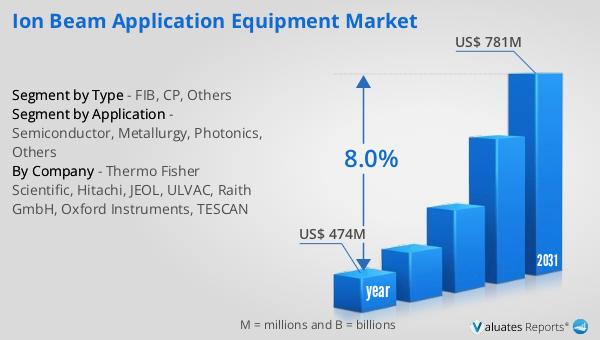
The global market for Ion Beam Application Equipment was valued at $474 million in 2024 and is anticipated to grow significantly, reaching an estimated size of $781 million by 2031. This growth is expected to occur at a compound annual growth rate (CAGR) of 8.0% over the forecast period. This upward trajectory reflects the increasing demand for advanced ion beam technologies across various industries, driven by the need for precision and control in material modification and analysis. As industries continue to evolve and innovate, the role of ion beam application equipment becomes increasingly important, offering solutions that enable the development of smaller, more efficient, and more powerful devices. The market's growth is supported by continuous advancements in ion beam technologies, as companies invest in research and development to enhance the capabilities and efficiency of these tools. This dynamic environment fosters competition and collaboration among key players, driving the market forward and ensuring that ion beam application equipment remains at the forefront of technological innovation. The projected growth of the market highlights the critical role that ion beam technologies play in modern manufacturing and research, supporting the development of new products and technologies across a wide range of industries.
| Report Metric | Details |
| Report Name | Ion Beam Application Equipment Market |
| Accounted market size in year | US$ 474 million |
| Forecasted market size in 2031 | US$ 781 million |
| CAGR | 8.0% |
| Base Year | year |
| Forecasted years | 2025 - 2031 |
| Segment by Type |
|
| Segment by Application |
|
| Production by Region |
|
| Consumption by Region |
|
| By Company | Thermo Fisher Scientific, Hitachi, JEOL, ULVAC, Raith GmbH, Oxford Instruments, TESCAN |
| Forecast units | USD million in value |
| Report coverage | Revenue and volume forecast, company share, competitive landscape, growth factors and trends |